

Blood compatibility material with micro nano coupling interface structure and its manufacturing method
A technology of blood compatibility and interface structure, which is applied in the fields of medical containers, anticoagulant treatment, and packaged food, etc. It can solve problems such as failure to reduce platelet adhesion, interference with the stability of the coagulation system itself, and anticoagulant shedding. Achieve good anticoagulant performance, wide application prospects, and reduce adhesion
- Summary
- Abstract
- Description
- Claims
- Application Information
AI Technical Summary
Problems solved by technology
Method used
Image

Examples
Embodiment 1
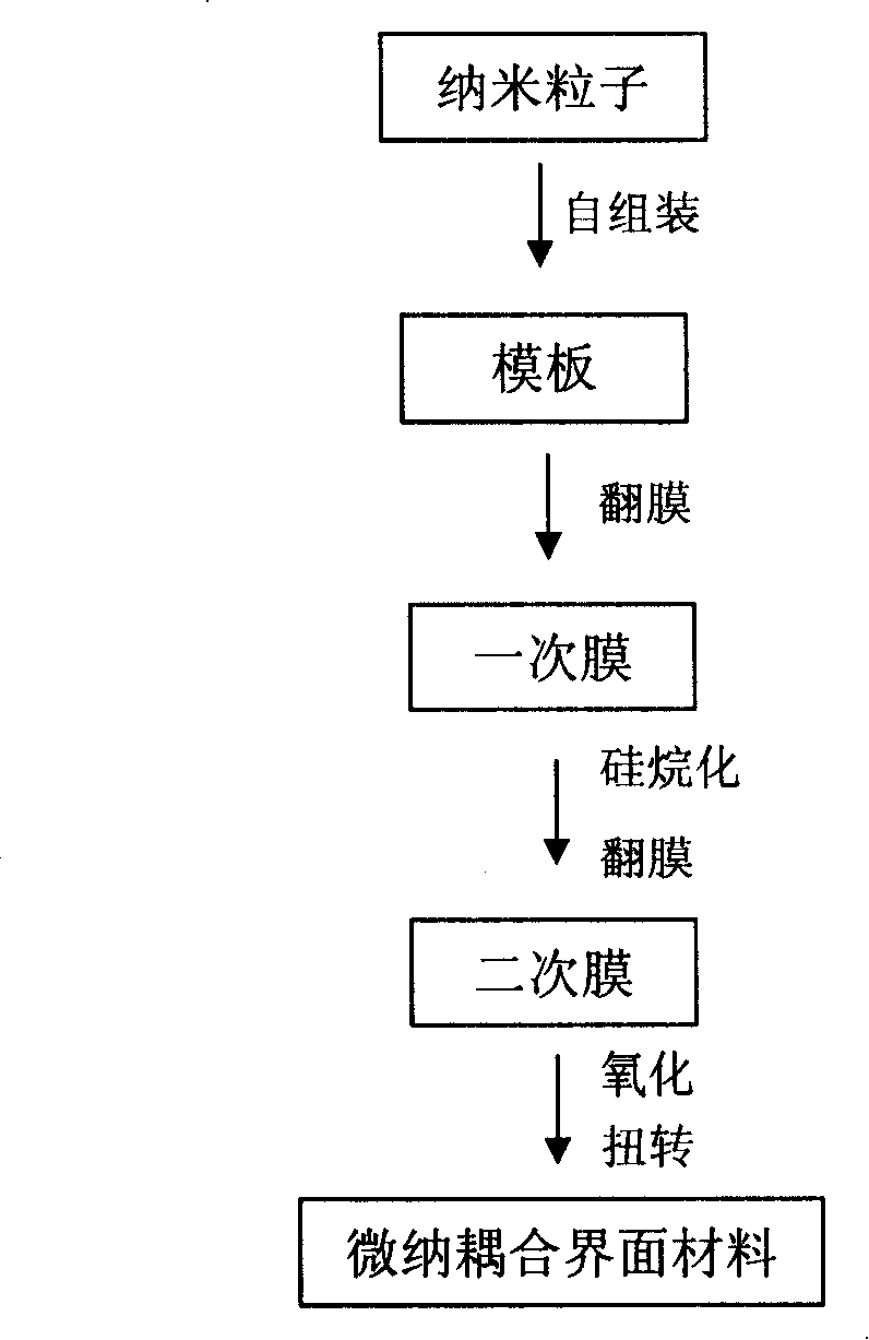
[0040] Polystyrene spheres with a particle size of 100nm were covalently self-assembled in a solution to form an initial template of polystyrene nanoparticles closely arranged on a silicon wafer.
[0041] Then cover the template with liquid polydimethylsiloxane (PDMS), keep it under room temperature and 60cmHg vacuum for 10 minutes, and then transfer it to an oven at 50°C for curing.
[0042] The cured polymer film was peeled off from the silicon wafer template, then soaked in the ethanol solution of perfluorosilane for 3 hours for hydrophobic treatment, and then dried naturally as a primary film.
[0043] Cover the primary film with liquid polydimethylsiloxane (PDMS), keep it under room temperature and 60cmHg vacuum for 20 minutes, then transfer it to an oven to cure at 70°C, and then peel it off from the primary film. form a secondary film.
[0044] The secondary film is cut into quadrilaterals, and the surface is attached to a cylinder with a diameter of 3 cm. The structur...
Embodiment 2
[0048] Silica spheres with a particle size of 100nm are covalently self-assembled in a solution to form an initial template of closely-arranged silica nanoparticles on a silicon wafer.
[0049] Cover the template with melted polytetrafluoroethylene, keep it under 380°C and 65cmHg vacuum for 20 minutes, and then slowly cool and solidify.
[0050] The cured polymer film was peeled off from the silicon wafer template, then soaked in polycarbosilane solution for 3 hours, and used as a primary film after hydrophobization treatment.
[0051] Pour melted polytetrafluoroethylene on the primary film, keep it under 380°C and 65cmHg vacuum for 20 minutes, then slowly cool and solidify, and then peel off from the primary film to form a secondary film.
[0052] Cut the secondary membrane into a quadrilateral, attach the surface to a cylinder with a diameter of 5 cm, expose the structured side (the side in contact with the primary membrane) to the air, and then oxidize it in a plasma cleane...
PUM
| Property | Measurement | Unit |
|---|---|---|
| Width | aaaaa | aaaaa |
| Width | aaaaa | aaaaa |
| Height | aaaaa | aaaaa |
Abstract
Description
Claims
Application Information