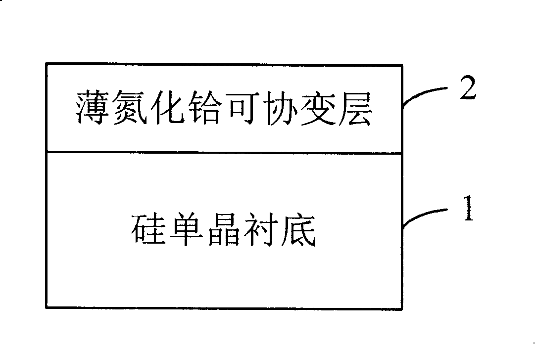
Silicon based compliant substrate material possessing thin hafnium nitride compliant layer
A substrate material, hafnium nitride technology, applied in lasers, electrical components, circuits, etc., to achieve the effect of reducing residual stress, good crystal quality, and avoiding impurity pollution problems
- Summary
- Abstract
- Description
- Claims
- Application Information
AI Technical Summary
Problems solved by technology
Method used
Image

Examples
Embodiment 1
[0056] Using ion beam epitaxy, a 90nm thick and 45nm thick covariable hafnium nitride layer (samples E1 and F1) 2 was prepared and grown on a Si(111) substrate 1, forming two covariable layers with different thicknesses. The silicon base of the layer can be a co-variable substrate.
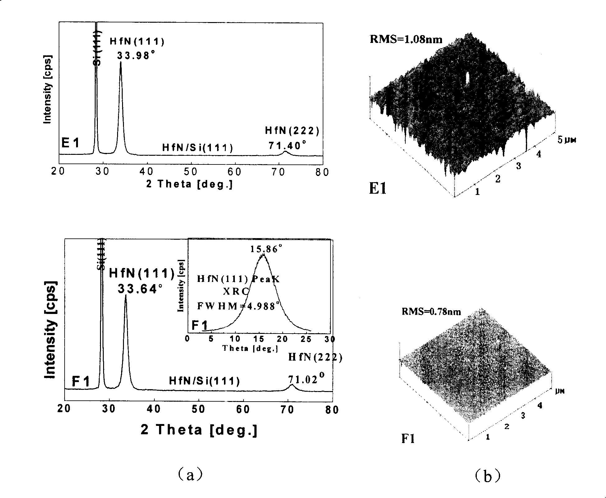
[0057] by figure 2 In (a) X-ray diffraction (XRD) and (b) atomic force surface topography test (AFM) test analysis results, it can be seen that the two thicknesses of thin hafnium nitride covariable layer 2 have cubic HfN (111 ) With a single preferred orientation, the surface is relatively smooth and flat. The root-mean-square roughness values of the AFM surface are 0.78nm and 1.08nm, respectively.
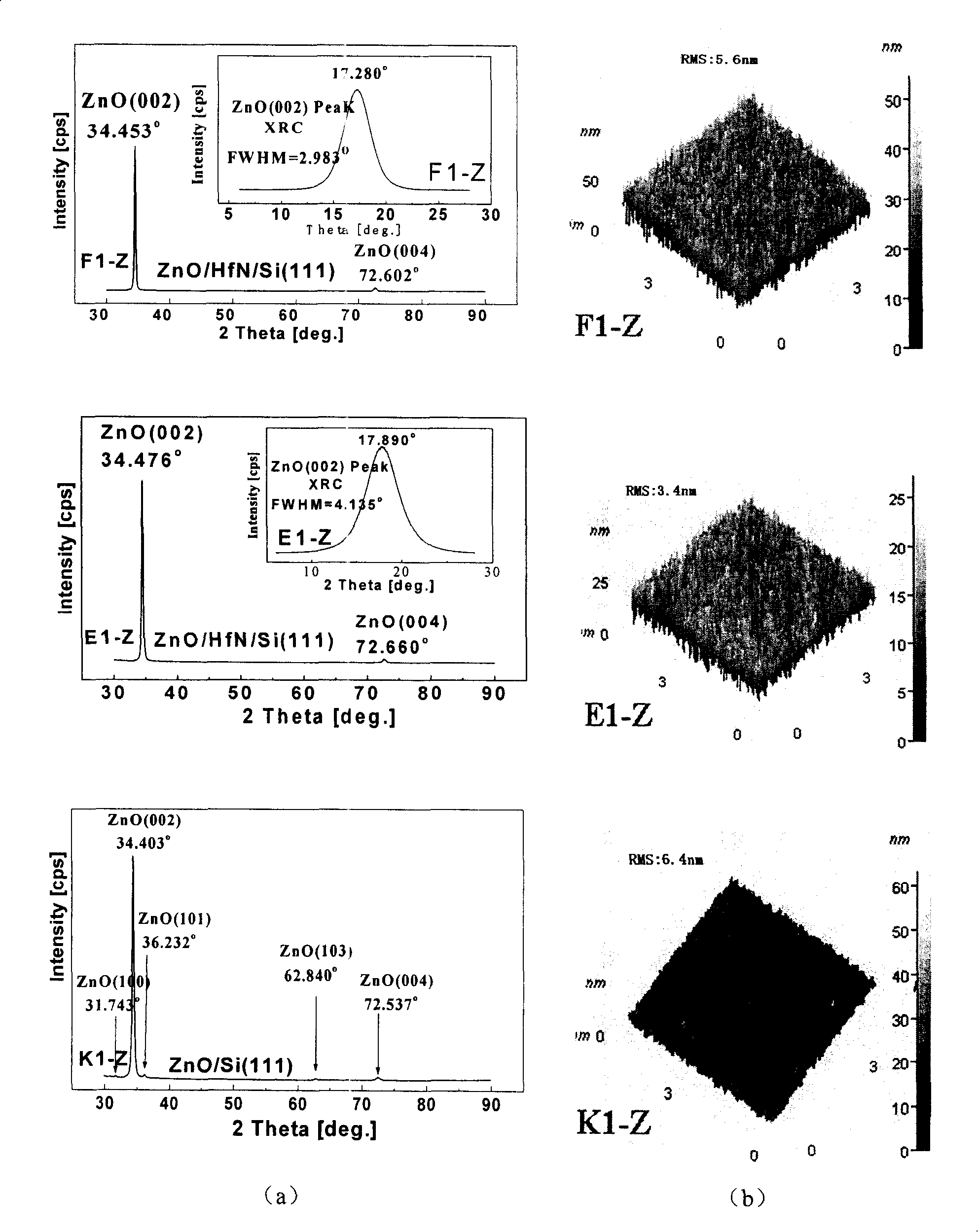
[0058] The same thickness of zinc oxide epitaxial film 3 is prepared by using the same magnetron sputtering process on these two kinds of silicon-based covariable substrates and ordinary Si(111) substrates.
[0059] by image 3 In (a) X-ray diffraction (XRD) test and analysis results can be seen: the ...
Embodiment 2
[0062] Using the ion beam epitaxy method, the 90nm thick and 18nm thick thin covariable hafnium nitride layers (samples E1 and F1) 2 grown on the Si (100) substrate 1 are formed, forming two coordinable layers with different thicknesses. The silicon-based variable layer can be a co-variable substrate.
[0063] by Figure 4 In (a) X-ray diffraction (XRD) and (b) atomic force surface topography test (AFM) test analysis results, it can be seen that the two thicknesses of thin hafnium nitride covariable layer 2 have cubic HfN (111 ) With a single preferred orientation, the surface is relatively smooth and flat. The root mean square roughness value of the G2 sample AFM is 0.20nm.
[0064] The same thickness of zinc oxide epitaxial film 3 is prepared by using the same magnetron sputtering process on these two kinds of silicon-based covariable substrates and ordinary Si(100) substrates.
[0065] by Figure 5 In (a) X-ray diffraction (XRD) test analysis results can be seen: the crystalline...
PUM
| Property | Measurement | Unit |
|---|---|---|
| thickness | aaaaa | aaaaa |
| thickness | aaaaa | aaaaa |
| particle size | aaaaa | aaaaa |
Abstract
Description
Claims
Application Information