Dielectric tunable film based on implantable nanowire electrode and its preparation method

A nanowire, implantable technology, applied in chemical instruments and methods, circuits, electrical components, etc., to achieve the effects of low loss, good application prospects, and fewer defects

Inactive Publication Date: 2011-12-21
ZHEJIANG UNIV
View PDF0 Cites 0 Cited by
  • Summary
  • Abstract
  • Description
  • Claims
  • Application Information

AI Technical Summary

Problems solved by technology

However, the modulation voltage of dielectric tunable films is usually between 25 and 100V, so there is still a lot of work to be done.

Method used


Image

  • Dielectric tunable film based on implantable nanowire electrode and its preparation method
  • Dielectric tunable film based on implantable nanowire electrode and its preparation method
  • Dielectric tunable film based on implantable nanowire electrode and its preparation method

Examples


Embodiment 1

[0034] 1) According to the chemical formula Pb x Sr 1-x TiO 3 , x=0.4, take powdered strontium carbonate, lead oxide and titanium dioxide, in which the lead oxide is over 0.02% mol to compensate for the volatilization loss of lead; mix by ball milling, then press the target, and sinter the target material Pb 0.4 Sr 0.6 TiO 3 ;

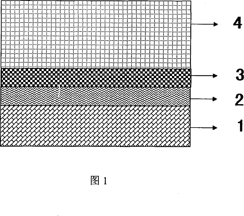
[0035] 2) Clean the glass substrate, and sequentially deposit Ti on the substrate by chemical vapor deposition 5 Si 3 Conductive film layer and TiSi conductive nanowire layer;

[0036] 3) Sputtering deposition of a dielectric film Pb on the titanium silicide conductive nanowire layer of the composite structure obtained in step 2) by magnetron sputtering 0.4 Sr 0.6 TiO 3 ; During sputtering, the vacuum degree of the reaction chamber was kept at 0.6Pa, with argon and oxygen as the sputtering atmosphere, the flow rates of argon and oxygen were 10sccm and 10sccm respectively, the sputtering power was 80W, and the sputtering time was 2h;

[0037] ...

Embodiment 2

[0040] 1) According to the chemical formula Pb x Sr 1-x TiO 3 , x = 0.1, take powdered strontium carbonate, lead oxide and titanium dioxide, in which the lead oxide is over 0.02% mol to compensate for the volatilization loss of lead; mix by ball milling, then press the target, and sinter the target material Pb 0.1 Sr 0.9 TiO 3 ;

[0041] 2) Clean the single crystal silicon substrate, and sequentially deposit Ti on the substrate by chemical vapor deposition 5 Si 3 conductive film layer and TiSi 2 conductive nanowire layer;

[0042] 3) Sputtering deposition of a dielectric film Pb on the titanium silicide conductive nanowire layer of the composite structure obtained in step 2) by magnetron sputtering 0.1 Sr 0.9 TiO 3 ; During sputtering, the vacuum degree of the reaction chamber was kept at 0.8Pa, with argon and oxygen as the sputtering atmosphere, the flow rates of argon and oxygen were 3sccm and 27sccm respectively, the sputtering power was 60W, and the sputtering ti...

Embodiment 3

[0046] 1) According to the chemical formula Pb x Sr 1-x TiO 3 , x=0.9, take powdered strontium carbonate, lead oxide and titanium dioxide, in which the lead oxide is over 0.02% mol to compensate for the volatilization loss of lead; mix by ball milling, then press the target, and sinter the target material Pb 0.9 Sr 0.1 TiO 3 ;

[0047] 2) Clean the polysilicon substrate, and deposit Ti sequentially on the substrate by chemical vapor deposition 5 Si 3 Conductive film layer and TiSi conductive nanowire layer;

[0048] 3) Sputtering deposition of a dielectric film Pb on the titanium silicide conductive nanowire layer of the composite structure obtained in step 2) by magnetron sputtering 0.9 Sr 0.1 TiO 3 ; During sputtering, the vacuum degree of the reaction chamber was kept at 1Pa, with argon and oxygen as the sputtering atmosphere, the flow rates of argon and oxygen were 12sccm and 45sccm respectively, the sputtering power was 90W, and the sputtering time was 2h;

[00...


PUM


Abstract

The dielectric adjustable thin film based on the implanted nanowire electrode disclosed by the present invention has a titanium silicide conductive thin film layer, a titanium silicide conductive nanowire layer and a dielectric thin film layer sequentially deposited on the substrate from bottom to top. The thin film can be prepared by magnetron sputtering deposition method or sol-gel method. The dielectric adjustable film based on the implanted nanowire electrode of the present invention implants titanium silicide conductive nanowires into the dielectric film, makes full use of the huge fringe electric field of the nanowire electrode, and can obtain very high dielectric strength at an extremely low modulation voltage. The tunability is much lower than the modulation voltage of the dielectric tunable film without nanowire electrodes, which is only 1 / 6 to 1 / 10 of the normal situation. The dielectric adjustable film based on the implanted nanowire electrode of the invention has good compactness, few defects and low loss. The dielectric film implanted with titanium silicide conductive nano-electrodes is a high-performance dielectric tunable film with high tunability and low loss, and has a good application prospect.

Description

technical field [0001] The invention relates to a dielectrically adjustable film based on an implanted nanowire electrode and a preparation method thereof. Background technique [0002] Since Iijima synthesized carbon nanotubes in 1991, one-dimensional nanomaterials have become a research hotspot in nanotechnology due to their novel physical, chemical and biological properties and potential applications in nanodevices. Based on nanowires, higher device density can be achieved that cannot be achieved by ordinary semiconductor technology. Therefore, with the development of nanotechnology and the miniaturization of microelectronic devices, the preparation of nanoelectronic and optoelectronic devices based on nanowires has caused Wide attention. They will play an important role in future integrated circuits, sensors, photodetectors, flat displays, and future nanocomputers. As far as silicide nanowires are concerned, it has attracted considerable attention from the internationa...

Claims


Application Information

Patent Timeline
Patent Type & Authority Patents(China)
IPC IPC(8): B32B33/00H01L29/00C23C28/04C23C14/08C23C14/58C23C14/35B32B17/06B32B9/00H01L21/28C23C16/42
Inventor 杜丕一胡安红翁文剑韩高荣赵高凌沈鸽宋晨路徐刚张溪文
Owner ZHEJIANG UNIV
Why Eureka
Try Eureka