Method for producing tiny soldered balls with repeatedly-usable substrates

A manufacturing method and substrate technology, applied in semiconductor/solid-state device manufacturing, electrical components, electrical solid-state devices, etc., can solve problems such as poor process controllability, easy introduction of various impurities, ineffective control of droplet size and continuous growth, etc. , to reduce production costs, avoid surface oxidation, wire drawing or fluffing, and avoid chipping, burrs and adhesion

Inactive Publication Date: 2008-08-20
SHANGHAI INST OF MICROSYSTEM & INFORMATION TECH CHINESE ACAD OF SCI
View PDF0 Cites 7 Cited by
  • Summary
  • Abstract
  • Description
  • Claims
  • Application Information

AI Technical Summary

Problems solved by technology

The main advantages of this method are good process controllability and high product yield, but it has obvious disadvantages at the same time: many preparation procedures, large equipment investment, high cost, and it is easy to introduce various ② The spray method is extended from the traditional powder preparation technology, which is characterized by strong production capacity but poor process controllability. In order to obtain solder balls in the required particle size range, it must go through multiple classification processes, which is easy to cause welding Oxidation and damage on the surface of the ball
The instillation method is to mold the molten metal with a fixed size. It is also characterized by strong production capacity, but the disadvantage is that it cannot effectively control the size and continuous growth of the droplets, and the solder balls have poor uniformity, low sphericity and surface oxidation.

Method used


Image

  • Method for producing tiny soldered balls with repeatedly-usable substrates

Examples


Embodiment Construction

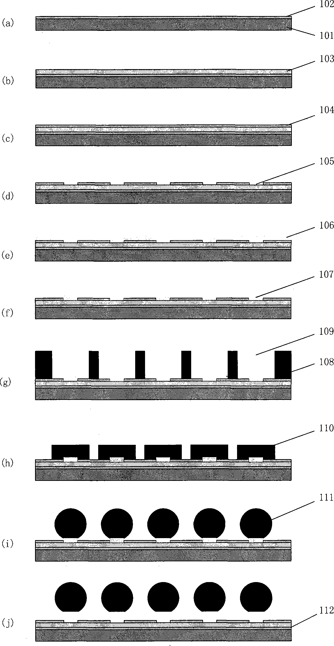
[0025] The preparation process flow of a typical micro solder ball includes the following steps:

[0026] 1. Using IC manufacturing process to prepare reusable substrates

[0027] (1) First, clean the single-side polished N-type (100) silicon wafer, and then perform thermal oxidation treatment, and the thickness of the silicon dioxide oxide layer 102 is about 0.3 microns;

[0028] (2) Vacuum sputtering metal conductive layer TiW and Au 103, the thickness is about 0.05 microns and 0.2 microns, respectively; the adhesion between the silicon dioxide layer and Au is poor, so TiW is used as the metal adhesion layer on the silicon dioxide , The three layers of metal are all sputtered sequentially in the same vacuum chamber;

[0029] (3) Then deposit a layer of barrier layer SiO on the conductive layer by plasma enhanced chemical vapor deposition (PECVD) method 2 Or Si 3 O 4 104, the thickness is about 0.1 micrometers; the circular barrier layer opening is etched by positive photoresist ...


PUM

PropertyMeasurementUnit
thicknessaaaaaaaaaa
thicknessaaaaaaaaaa
thicknessaaaaaaaaaa

Abstract

The invention relates to a method for manufacturing a small solder ball, in which a substrate is reusable. The invention is characterized in: firstly, the reusable substrate is prepared by means of IC manufacture process: a silicon wafer is used as a base, a metal conducting layer is sputtered from the front after heat oxidation treatment; secondly, the small solder ball is manufactured on the reusable substrate: a metal sacrificial layer is sputtered on the substrate to cover the opening of the conducting layer, thick photosensitive resist is coated and an electroplating window is photoetched, then solder is electroplated, the thick photosensitive resist is removed after electroplating, the solder is reflowed to form a solder ball, thereafter the metal sacrificial layer is corroded to be removed, so that the solder ball can drop off completely from the reusable substrate, and finally the solder ball is collected. According to the invention, the manufacturing procedure is simple and consumes small energy, the process has good controllability, the bottleneck of low productivity is overcome; the manufactured solder ball has smooth surface, good sphericity and uniform size, with the smallest grain diameter being 0.15mm.

Description

Technical field [0001] The invention relates to a method for preparing micro solder balls with a reusable substrate, which belongs to the field of electronic packaging. Background technique [0002] With the rapid development of consumer electronic products in the direction of "light, thin, short, small" and multi-functional, higher requirements are put forward on electronic assembly technology, forcing packaging technology to high-density, miniaturization, and integration. Evolution of direction. New high-density packaging technologies continue to emerge, and area array packaging forms such as Ball Grid Array (BGA) and Chip Scale Package (CSP) are the mainstream of future high-density packaging technologies. In the BGA and CSP packaging process, the replacement of pins with precision solder balls to achieve electrical and mechanical connections between the circuit substrate and the chip has become a key material for electronic packaging. Advanced electronic packaging has very st...

Claims


Application Information

Patent Timeline
Patent Type & Authority Applications(China)
IPC IPC(8): H01L21/60
CPCH01L2224/11
Inventor 林小芹罗乐
Owner SHANGHAI INST OF MICROSYSTEM & INFORMATION TECH CHINESE ACAD OF SCI
Why Eureka
Try Eureka