High flux test chip of single cell traveling wave dielectric spectrum and test method

A test method and technology of dielectric spectrum, which is applied in the high-throughput test chip and test field of single-cell traveling wave dielectric spectrum, can solve the problems of inability to realize large-scale parallel testing, small number of test samples, and small moving range of optical tweezers, etc. problems, to achieve the effect of compact structure, easy integration, and fewer chip pins

Inactive Publication Date: 2008-10-01
SOUTHEAST UNIV
View PDF0 Cites 8 Cited by
  • Summary
  • Abstract
  • Description
  • Claims
  • Application Information

AI Technical Summary

Problems solved by technology

[0007] Technical problem: The purpose of the present invention is to provide a high-throughput test chip and test method for single-cell traveling-wave dielectric spectrum, which can make each single cell to be tested produce its own independent dielectric response, and then realize high-throughput parallel testing. To solve the current cell dielectric response testing technology's difficulty in automatic detection of cells with a circularly symmetrical optical appearance, the small number of samples for each test, and the small movement range of optical tweezers that cannot achieve large-scale parallel testing

Method used


Image

  • High flux test chip of single cell traveling wave dielectric spectrum and test method
  • High flux test chip of single cell traveling wave dielectric spectrum and test method
  • High flux test chip of single cell traveling wave dielectric spectrum and test method

Examples


Embodiment Construction

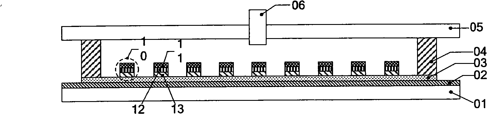
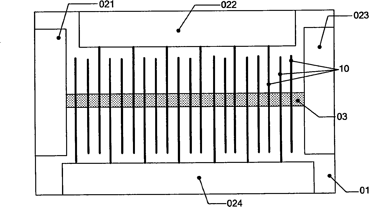
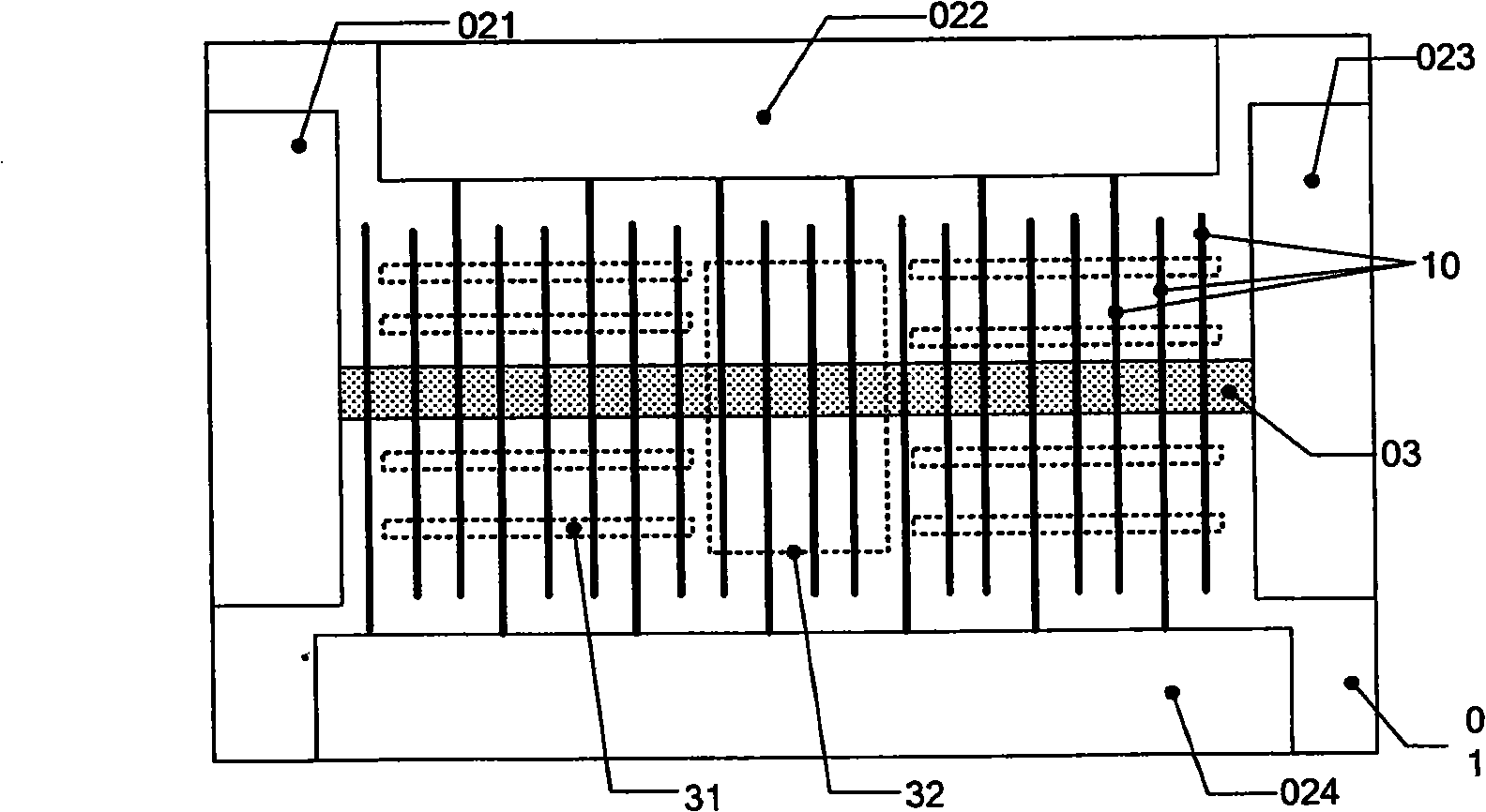
[0023] The embodiment of the high-throughput test chip of single-cell traveling wave dielectric spectrum provided by the present invention is as follows: figure 1 and figure 2As shown, it includes a microelectrode group 10 , a chip substrate 01 , a conductive layer 02 , an insulating layer 03 with via holes, a chip middle spacer layer 04 , a chip cover sheet 05 and an injection port 06 . The microelectrode group 10 is divided into three layers: an intrinsic photoconductive layer 11 , an n+ type photoconductive layer 12 and a transparent conductive film layer 13 . The material of the intrinsic photoconductive layer 11 can be selected from intrinsic state hydrogenated amorphous silicon; the material of the n+ type photoconductive layer 12 can be selected from n+ type hydrogenated amorphous silicon; the material of the transparent conductive film layer 13 can be selected from indium tin oxide transparent film material ; The width of the electrode should generally be more than 1...


PUM


Abstract

A method for testing a high-pass test chip of the single-cell travelling wave dielectric spectrum comprises the following procedures: respectively connecting each terminal of the test chip to the source end of the sinusoidal voltage signal which has same frequency to lead to that the advance mount or hysteresis amount of the phase between random two adjacent electrodes is equal, dripping the liquid sample containing the cell to be tested into the inner part of the test chip from the injection port (06), then projecting light pattern to the cell initial collection area (32) at the central areaof the electrode group (10), projecting a plurality of strip light patterns (31) with width about the cell diameter from the lower part of the chip substrate (01) to the microelectrode group (10) to form a virtual electrode array, regulating the frequency of a waveform generator, and at the same time recording the horizontal moving image of all cells in the frequency band through a CCD and an image recorder on a microscope. If the cell number of the completed test actually has already satisfied the requirement of the test, then the test procedure ends.

Description

technical field [0001] The invention relates to the parallel testing technology of single-cell dielectric response and the manipulation technology of micro-nano particles. Background technique [0002] According to the Maxwell-Wagner interface polarization theory, cells will be passively polarized under the condition of an external AC electric field, causing the dielectric relaxation phenomenon of cells. The dielectric constant ε and electrical conductivity σ of cells can be obtained analytically based on the characteristics of dielectric relaxation and the passive characteristics of cells in the frequency domain (or dielectric spectrum). The research on the frequency-domain passive characteristics of cells has become one of the research hotspots in cell electrophysiology and cell biophysics. Determining the dielectric response spectrum of a cell in the frequency domain enables characterization of the cell. [0003] At present, the methods for obtaining the dielectric prop...

Claims


Application Information

Patent Timeline
Patent Type & Authority Applications(China)
IPC IPC(8): G01N33/48C12Q1/02A61B5/00A61B10/00
Inventor 朱晓璐易红倪中华
Owner SOUTHEAST UNIV
Why Eureka
Try Eureka