Method for producing nano-structure on insulated underlay

A nanostructure technology on an insulating substrate, which is applied in the direction of optomechanical equipment, pattern surface photolithography, semiconductor/solid-state device manufacturing, etc. It can solve problems such as pollution, sample contamination, and change of material properties, and achieve assisted dissolution The effects of craftsmanship, precise implementation, and increased flexibility

Inactive Publication Date: 2008-10-29
INST OF PHYSICS - CHINESE ACAD OF SCI
View PDF0 Cites 21 Cited by
  • Summary
  • Abstract
  • Description
  • Claims
  • Application Information

AI Technical Summary

Problems solved by technology

Although this method can effectively avoid the accumulation of charges in electron beam exposure, if the conductive layer material on the surface of the substrate is not effectively removed, it may cause contamination of the sample and even change the characteristics of the material, such as Conductive layers such as ITO glass can only be removed by etching, which increases the complexity of the process and may cause damage to the pattern
Moreover, the two methods mentioned above simply solve the problem of electron beam exposure on the insulating substrate, which is not only helpful to the subsequent stripping process, but also often accompanied by serious side effects, such as high accelerating voltage. Severe edge effects or cracking of the electronic resist layer, without any treatment, simply plating a conductive layer on the surface of the substrate or resist layer will often bring unnecessary pollution or have to introduce unnecessary Etching process

Method used


Image

  • Method for producing nano-structure on insulated underlay
  • Method for producing nano-structure on insulated underlay

Examples


Embodiment 1

[0031] Embodiment 1, the method for making nanostructures on insulating quartz glass, comprising the following steps:

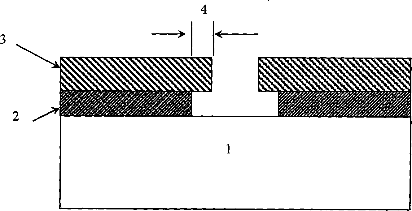
[0032] 1. Select insulating quartz glass as the substrate, select 0.8mm double-sided polished quartz glass as substrate 1, and use acetone, alcohol and deionized water in sequence, after ultrasonic cleaning, dry with dry nitrogen, and put it at 95 ℃ Bake on the hot plate for two hours and set aside;

[0033] 2. Using thermal evaporation coating equipment, deposit a layer of 80nm aluminum film 2 on the above baked quartz glass substrate 1, and then spin-coat a layer of electron beam resist with a thickness of about 140nm on the aluminum film 2 Agent 3, the electron beam resist is made of PMMA 495 glue purchased on the market, and the spin coating speed is 4000 rpm; after spin coating, a hot plate at 180°C is used to pre-bake the sample, and the pre-baking time is 65 seconds;

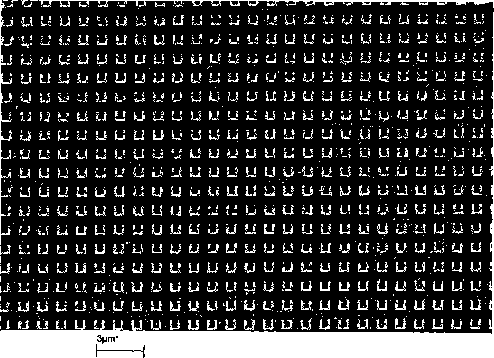
[0034] 3 Design of nanostructure pattern: According to the size and shape of the U-...

Embodiment 2

[0041] The preparation method of the present embodiment is the same as in Example 6, except that the conditions are as follows:

[0042] Fabrication of nano-copper electrodes on substrate 1 of insulating sapphire: 1 mm thick double-sided polished sapphire was cleaned by ultrasonic with acetone, alcohol and deionized water, dried with dry nitrogen, and then baked on a hot plate at 115 °C for two hours . A layer of 120nm aluminum film 2 was deposited on the sapphire substrate using magnetron sputtering coating equipment, and then a layer of electron beam resist 3 with a thickness of about 120nm was spin-coated on the aluminum film 2. The electron beam resist Use commercially available PMMA950 glue. After spin coating, the samples were pre-baked in an oven at 180°C for 30 minutes. The sample was then exposed using an electron beam exposure system. Exposure patterns were edited by GDSII software, including line structures with a minimum line width of 60 nm. Exposure parameters...

Embodiment 3

[0044] The preparation method of the present embodiment is the same as in Example 6, except that the conditions are as follows:

[0045] Fabrication of nano-gold electrodes on substrate 1 of insulating glass: After cleaning the 0.5 mm thick glass substrate with acetone, alcohol and deionized water with ultrasonic and blowing it dry with dry nitrogen, bake it on a hot plate at 180°C for 20 years. minute. A layer of 60nm aluminum film 2 was deposited on the sapphire substrate using magnetron sputtering coating equipment, and then a layer of electron beam resist 3 with a thickness of about 200nm was spin-coated on the aluminum film. Commercially available ZEP520 glue. After spin coating, the samples were pre-baked on a hot plate at 200°C for 2 minutes. The sample was then exposed using an electron beam exposure system. The exposure pattern is edited by L-edit software, including the line structure with a minimum line width of 80nm and a minimum line spacing of 150nm. Exposure...


PUM

PropertyMeasurementUnit
widthaaaaaaaaaa
thicknessaaaaaaaaaa
thicknessaaaaaaaaaa

Abstract

The invention relates to a method for preparing nanometer structures on an insulating substrate. The method comprises the following steps of: selecting and disposing the insulating substrate; spin-coating electronic anti-corrosion adhesive after an aluminium film with suitable thickness is aggraded on the substrate by coating equipment; designing the shape and the dimension of the required surface nanometer structure according to the requirement; realizing the precise exposal of the design graphics on the surface of the substrate in an electron beam exposal system; realizing suitable undercut structure at the exposal line position in a dual-layer structure of electronic anti-corrosion adhesive and aluminium by controlling the process parameters such as temperature of alkali liquor, consistency of alkali liquor and corrosion disposal time; finally realizing the sediment of nanometer structure material by the coating equipment and completing the preparation of the nanometer structure by solubilisation process and alkali liquor disposal. The method overcomes the charge accumulation effect of the insulating substrate in the electron beam exposal system and realizes the exposal of the nanometer graphics; meanwhile, the prepared undercut structure can extremely effectively assist the subsequent solubilisation process, thus ensuring that the surface nanometer structure is effectively, integrally and precisely realized on the insulating substrate material.

Description

technical field [0001] The invention relates to a manufacturing method for realizing nanostructures on insulating substrates, in particular to a manufacturing method for preparing metal nanostructures on insulating substrate materials by applying electron beam exposure technology. Background technique [0002] Subwavelength-sized artificial materials with special electromagnetic propagation properties, such as high-frequency magnetically responsive materials, left-handed materials, etc., have been the focus of close attention in recent years. This material is usually realized by fabricating subwavelength-sized metallic artificial structures on the surface of the substrate medium. Therefore, in order to realize the application in the near-infrared and visible light bands, it is necessary to realize sub-micron or nano-scale artificial structures on the substrate. Using electron beam exposure technology, sub-micron or nano-scale pattern transfer can be achieved on substrates w...

Claims


Application Information

Patent Timeline
Patent Type & Authority Applications(China)
IPC IPC(8): G03F7/00H01L21/027G06F17/50
Inventor 顾长志夏晓翔杨海方李俊杰罗强金爱子
Owner INST OF PHYSICS - CHINESE ACAD OF SCI
Why Eureka
Try Eureka