Method for manufacturing photoelectricity semiconductor element of semiconductor containing P-type three-tribe nitrogen compound

A technology of optoelectronic semiconductors and manufacturing methods, applied in the direction of semiconductor/solid-state device manufacturing, semiconductor devices, electrical components, etc., can solve the damage of epitaxial layer, do not meet the requirements of equipment cost and output efficiency, and increase the steps of heating and cooling And other issues

Inactive Publication Date: 2011-04-06
ZHANJING TECH SHENZHEN +1
View PDF2 Cites 0 Cited by
  • Summary
  • Abstract
  • Description
  • Claims
  • Application Information

AI Technical Summary

Problems solved by technology

[0008] Both of the above two methods of activating doped magnesium have many disadvantages: Toyoda Gosei uses low-energy electron beams to produce P-type gallium nitride, so it does not meet the requirements of mass production equipment cost and output efficiency
Therefore, not only the steps of heating and cooling are added to make the process complicated and time-consuming, but also the epitaxial layer will be damaged due to rising to high temperature, which means that the light-emitting quality of the light-emitting diode will be reduced.

Method used


Image

  • Method for manufacturing photoelectricity semiconductor element of semiconductor containing P-type three-tribe nitrogen compound
  • Method for manufacturing photoelectricity semiconductor element of semiconductor containing P-type three-tribe nitrogen compound
  • Method for manufacturing photoelectricity semiconductor element of semiconductor containing P-type three-tribe nitrogen compound

Examples


Embodiment Construction

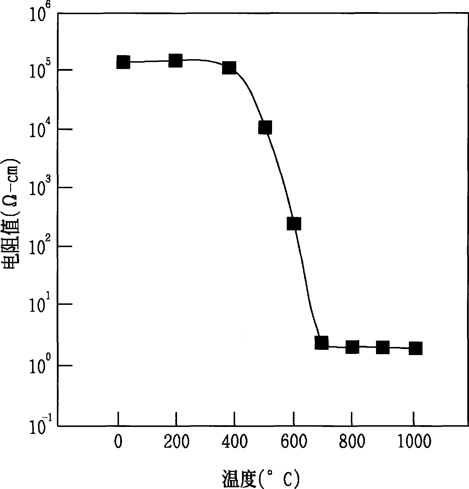
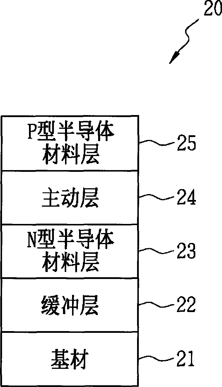
[0017] figure 2 It is a structural diagram of an optoelectronic semiconductor element containing P-type III nitrogen compound semiconductor. Generally speaking, to manufacture the light-emitting diode 20, a substrate 21 is firstly provided, such as sapphire (that is, aluminum oxide compound Al 2 o 3 ), and different material layers are formed on the substrate 21. Because the lattice constants of the substrate 21 and the III-nitride compound do not match, at least one buffer layer 22 , such as aluminum nitride (AlN) or gallium nitride (GaN), needs to be formed on the substrate 21 first. Then, an N-type semiconductor material layer 23 is grown on the buffer layer 22 , and an N-type GaN-doped silicon film can be produced by epitaxy as the N-type semiconductor material layer 23 . Then grow an active layer 24 of a multilayer quantum well structure on the N-type semiconductor material layer 23, such as a five-layer indium gallium nitride (InGaN) / gallium nitride (GaN) multilayer ...


PUM


Abstract

A manufacturing method of a photoelectric semiconductor element containing a P-type group III nitride semiconductor comprises allowing a reacting gas containing a P-type dopant to grow on a substrate to obtain a group III nitride semiconductor; reducing the temperature in a reaction chamber to 700-850 DEG C, introducing nitrogen gas or an inert gas to discharge ammonia and hydrogen out of the reaction chamber, and reducing the pressure in the reaction chamber to 20-80 kPa; keeping for a sufficient time until the residual ammonia and hydrogen are completely discharged, reducing the temperaturein the reaction chamber to room temperature, and taking out the substrate.

Description

technical field [0001] The invention relates to a method for manufacturing an optoelectronic semiconductor element containing P-type III-group nitrogen compound semiconductor, in particular to a method for activating P-type dopant in the III-group nitrogen compound semiconductor. Background technique [0002] As light-emitting diode elements are widely used in different products, in recent years, materials for making blue light-emitting diodes have become an important research and development object in the current optoelectronic semiconductor material industry. At present, the materials of blue light-emitting diodes include zinc selenide (ZnSe), silicon carbide (SiC) and indium gallium nitride (InGaN). above eV. [0003] Since the gallium nitride series is a light-emitting material with a direct gap, it can produce high-brightness illumination light, and has the advantage of longer life than zinc selenide, which also has a direct gap. In addition, the energy gap of gallium...

Claims


Application Information

Patent Timeline
Patent Type & Authority Patents(China)
IPC IPC(8): H01L33/00H01L21/18
Inventor 黄世晟涂博闵叶颖超徐智鹏詹世雄
Owner ZHANJING TECH SHENZHEN
Why Eureka
Try Eureka