Nanocrystal iron nitride thin-film material and functions thereof

An iron nitride and nanocrystalline technology, applied in the application of magnetic film to substrate, metal material coating process, cathode sputtering application, etc., can solve the problems of large size, poor conductivity and low operating temperature of Hall devices , to achieve the effect of small size, good linearity and low cost

Inactive Publication Date: 2009-09-02
NANKAI UNIV
View PDF2 Cites 11 Cited by
  • Summary
  • Abstract
  • Description
  • Claims
  • Application Information

AI Technical Summary

Problems solved by technology

[0007] In order to solve the problems of large volume, low operating temperature, and poor conductivity of the Hall device with semiconductor film as the magnetically sensitive active layer, a material for the magnetically sensitive layer of the Hall device that is more economical and practical and can maintain linearity in a larger magnetic field range is sought. , the present invention provides a brand-new nanoscale polycrystalline iron nitride Fe that can be used as an active layer material x N(2

Method used


Image

  • Nanocrystal iron nitride thin-film material and functions thereof
  • Nanocrystal iron nitride thin-film material and functions thereof
  • Nanocrystal iron nitride thin-film material and functions thereof

Examples


Embodiment 1

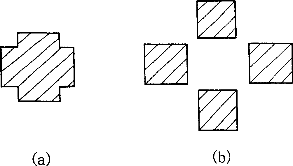
[0032] 1. Preparation of active layer pattern. Form a "cross" pattern on a quartz substrate for depositing an iron nitride film by using a mask method, such as figure 1 (a) shown. There is no photoresist in the shaded part of the figure, the side length of the central square of the pattern is 1.0 μm, and the length of the protruding part on the four sides of the central square is 0.2 μm;

[0033] 2. Admit argon gas at room temperature. The DPS-III type ultra-high vacuum magnetron sputtering coating machine (built-in computer control software) of the Shenyang Keyi Center of the Chinese Academy of Sciences is adopted, and the vacuum degree of the back and the bottom is less than 3.0×10 -5 Pa, the high-purity Ar gas and N 2 The gas mixture is passed into the vacuum chamber. Where the Ar gas flow rate is 10sccm, N 2 The air flow is 2 sccm. When the vacuum degree drops to about 0.1Pa, use the computer control software that comes with the equipment to set the opening degree of...

Embodiment 2

[0042] 1. The preparation of the active layer pattern is the same as step 1 of Example 1;

[0043] 2. Adopt the DPS-III type ultra-high vacuum magnetron sputtering coating machine (built-in computer control software) of the Shenyang Keyi Center of the Chinese Academy of Sciences, and the vacuum degree at the back and the bottom is better than 3.0×10 -5 Pa, the high-purity Ar gas and N 2 The gas mixture is passed into the vacuum chamber. Where the Ar gas flow rate is 6 sccm, N 2 The air flow is 1 sccm. When the vacuum degree drops to about 0.1Pa, use the computer control software that comes with the equipment to set the opening degree of the ultra-high vacuum gate valve to 20%;

[0044] 3. Apply a radio frequency power of 50W to the iron target with a purity of 99.99%, and pre-sputter for 10 minutes;

[0045] 4. Open the baffle of the quartz substrate, the substrate rotates at a constant speed of 20 rpm, and the sputtering time is controlled at 30 minutes;

[0046] 5, the ...

Embodiment 3

[0053] 1. The preparation of the active layer pattern is the same as step 1 of Example 1;

[0054] 2, feed argon gas at room temperature with step 2 of embodiment 1;

[0055] 3, pre-sputtering is the same as step 3 of embodiment 1;

[0056]4. Sputtering film formation. Open the baffle of the quartz substrate, the substrate rotates at a constant speed of 20 rpm, and the sputtering time is controlled to be 1 minute, 10 minutes and 30 minutes respectively, and samples I, II and III are obtained;

[0057] 5, the preparation method of electrode is the same as embodiment 1 step 5;

[0058] 6, the preparation method of protective layer is the same as embodiment 1 step 6;

[0059] Dektak3 surface topography instrument was used to measure the thickness of the active layer of the iron nitride film of Hall element I, II and III respectively, and the measurement results are listed in Table 1;

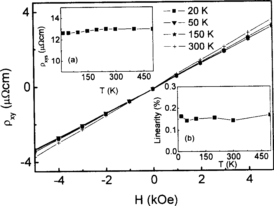
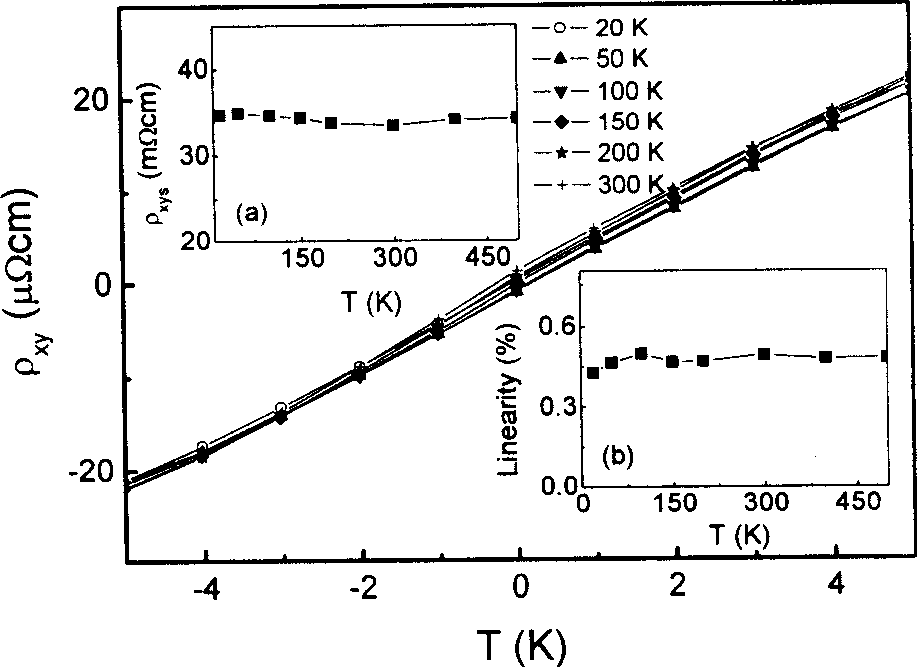
[0060] Using the physical property measuring instrument PPMS-9 produced by Quantum Design C...


PUM

PropertyMeasurementUnit
thicknessaaaaaaaaaa
thicknessaaaaaaaaaa
thicknessaaaaaaaaaa

Abstract

The invention relates to a thin-film material and a preparation method thereof, in particular to an iron nitride thin-film material which can be applied to a magnetic sensitivity active layer of Hall elements and a preparation method thereof. The general formula of the nanocrystal iron nitride thin-film material is FexN, wherein x is the atom number ratio between the iron and the nitrogen contained in the material and x is larger than 2 and less than 4; the thickness of the thin-film is between 4 nanometers and 400 nanometers; compared with the traditional thin-film made of semiconductor materials and particles, the nanocrystal iron nitride thin-film has the advantages of low resistivity, wide operating temperature range, excellent linearity and small volume, and simple preparation process and low cost, thus having a wide range of application prospect in the fields of aviation, astronavigation, military and the like.

Description

technical field [0001] The present invention relates to a kind of film material and preparation method thereof, especially a kind of Fe that can be applied to the magnetically sensitive active layer of Hall element x N(2<x<4) thin film material and its preparation method. Background technique [0002] The Hall element is a magnetic sensor device that uses the Hall effect of the active layer material to measure the magnetic field. It consists of an active layer, electrodes and a package that protects them. At present, the annual demand for Hall devices in the world is more than 1 billion, and they have been used in brushless motors, gear speed detection, non-contact switches and positioning switches in process control, and automotive safety devices ABS (anti-lock braking system). dynamic system), automotive engine ignition timing, current and voltage sensors, etc. have been widely used. It is characterized by non-contact sensing, high reliability, used to detect curre...

Claims


Application Information

Patent Timeline
Patent Type & Authority Applications(China)
IPC IPC(8): H01F10/18H01F41/18C23C14/35C23C14/04C23C14/06C23C14/54
Inventor 刘晖程雅慧
Owner NANKAI UNIV
Why Eureka
Try Eureka