Nano composite phase-change material and preparation method thereof
A phase change material and nanocomposite technology, which is applied in the field of nanocomposite phase change materials and its preparation, can solve problems such as the influence of C-RAM device reliability, improve data retention capabilities, enhance dielectric properties and breakdown resistance, The effect of increasing heat capacity
- Summary
- Abstract
- Description
- Claims
- Application Information
AI Technical Summary
Problems solved by technology
Method used
Image
Examples
preparation example Construction
[0028] For the preparation of phase change composite materials, we can adopt the mixed preparation method of phase change materials and ferroelectric materials, and mix the phase change materials and ferroelectric materials evenly, so that the ferroelectric materials can evenly disperse the phase change materials into nanometer particles with uniform size and shape. size region, thereby limiting the reversible phase change of phase change materials to a tiny region.
[0029] In the material preparation process, the ferroelectric material is compounded in the phase change material, and the phase change material is evenly divided into regions with controllable size and shape by the ferroelectric material, so that the phase change of the phase change material is limited to a small area, and the growth of its grains is prevented. big. After the ferroelectric material is introduced, the obtained composite material maintains the original reversible phase transition characteristics. ...
Embodiment
[0038] Preparation of nanocomposite phase change materials—Ge by magnetron sputtering 2 Sb 2 Te 5 with Ba 0.5 Sr 0.5 TiO 3 complex.
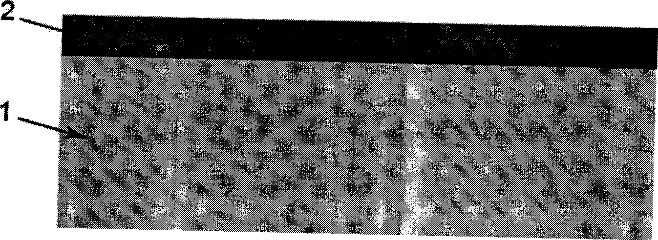
[0039] 1) Clean two (100) oriented silicon substrates, prepare a 100nm thick tungsten electrode 2 on one of the silicon substrates 1, as Figure 1a shown.
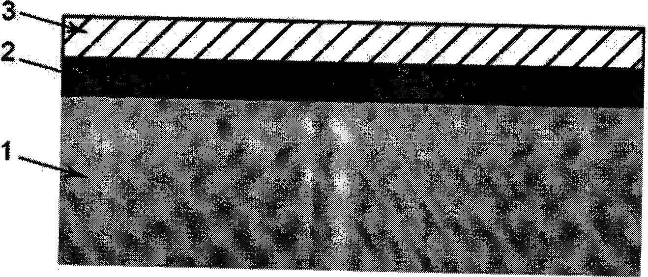
[0040] 2) Deposit a silicon oxide layer 3 on the substrate with tungsten electrodes again, with a thickness of 100nm, such as Figure 1b shown.
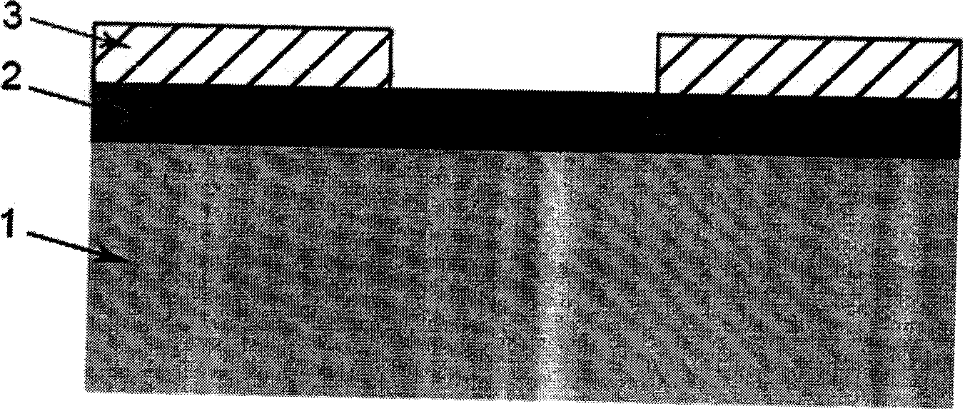
[0041] 3) A small hole with a diameter of 200nm is carved on the silicon oxide by using the exposure-etching process. The exposure method used is electron beam exposure, and the etching method is reactive ion etching. The structure is as follows: Figure 1c shown.
[0042] 4) Prepare the nanocomposite phase change material 4 on the silicon substrate and the silicon substrate with tungsten electrodes. Using Ge 2 Sb 2 Te 5 alloy target and Ba 0.5 Sr 0.5 TiO 3 Thin films were prepared by simultaneous sputtering of two targets. During ...
PUM
| Property | Measurement | Unit |
|---|---|---|
| thickness | aaaaa | aaaaa |
Abstract
Description
Claims
Application Information


