

Au-ZnO two-dimensional photon crystal structure and preparation method thereof
A two-dimensional photonic crystal and crystal structure technology, applied in the direction of microsphere preparation, crystal growth, chemical instruments and methods, etc., can solve the problems of environmental pollution, high cost, low processing efficiency, etc., and achieve improved control performance, low cost, The effect of reducing equipment requirements
- Summary
- Abstract
- Description
- Claims
- Application Information
AI Technical Summary
Problems solved by technology
Method used
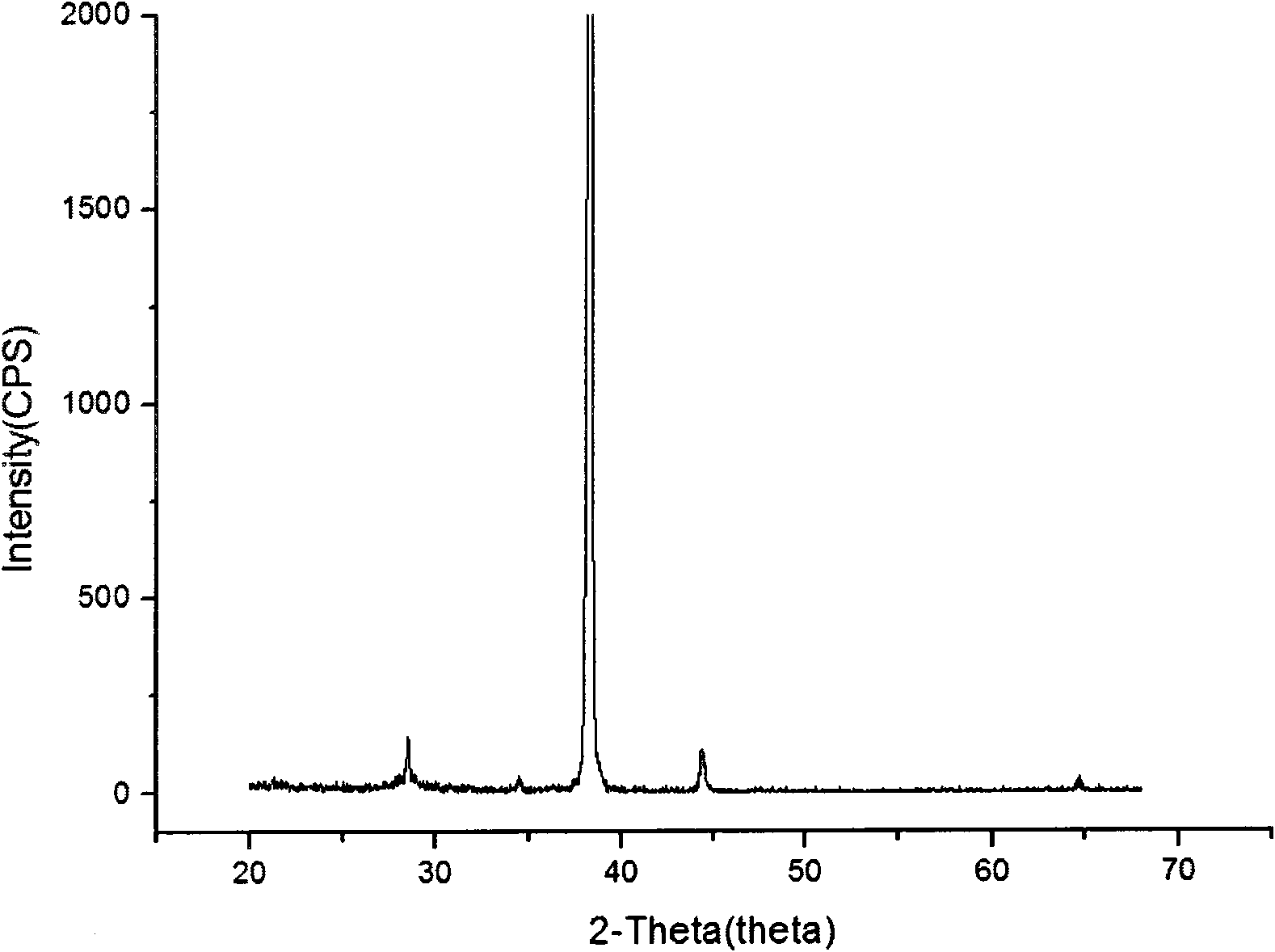
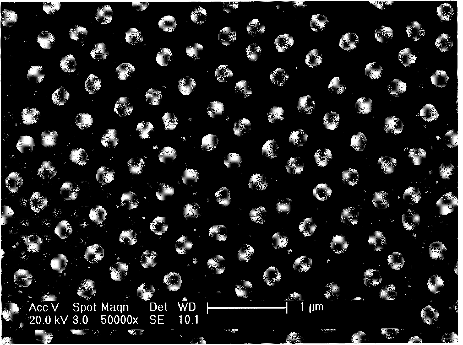
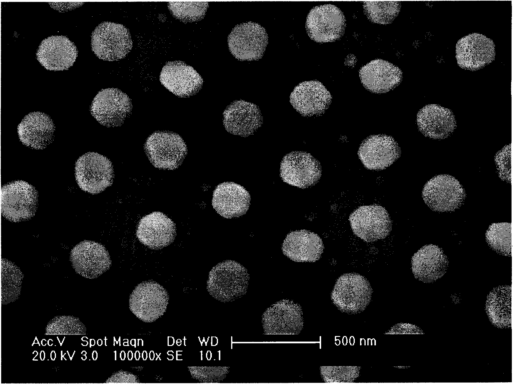
Image

Examples
Embodiment 1
[0019] a), making a single-layer polystyrene ball template
[0020] Clean the silicon wafer, put it vertically into the suspension of polystyrene beads with a mass fraction of 0.1% after being ultrasonicated for 3 hours, and put it into an electric constant temperature blast drying oven for 3 days at a temperature of 50°C to obtain a template;
[0021] b), making patterned Au catalyst
[0022] Put the template obtained in step a into a small ion sputtering apparatus, spray Au on it, control the power at 2W, and take 200s; then put the template in a quartz boat, and put the quartz boat into a level that has been heated to 500°C in advance In the tubular growth furnace, keep at 500°C for 1 hour, take out the quartz boat, and take out the template;
[0023] c), growing Au-ZnO two-dimensional photonic crystal structure
[0024] Grind ZnO and carbon powder evenly with a mass ratio of 1:2, put them in a quartz boat as an evaporation source, then insert the template obtained in ste...
Embodiment 2
[0026] a), making a single-layer polystyrene ball template
[0027] Clean the silicon wafer, put it vertically into the suspension of polystyrene beads with a mass fraction of 0.2% after being ultrasonicated for 5 hours, and put it into an electric constant temperature blast drying oven for 4 days at a temperature of 30°C to obtain a template;
[0028] b), making patterned Au catalyst
[0029] Put the template obtained in step a into a small ion sputtering apparatus, spray Au on it, control the power at 3W, and put the template into a quartz boat, and put the quartz boat into a level that has been heated to 450°C in advance In the tubular growth furnace, keep at 450°C for 1.5 hours, take out the quartz boat, and take out the template;
[0030] c), growing Au-ZnO two-dimensional photonic crystal structure
[0031] Grind ZnO and carbon powder evenly with a mass ratio of 2:3, put them in a quartz boat as an evaporation source, then insert the template obtained in step b vertica...
PUM
| Property | Measurement | Unit |
|---|---|---|
| quality score | aaaaa | aaaaa |
| quality score | aaaaa | aaaaa |
| quality score | aaaaa | aaaaa |
Abstract
Description
Claims
Application Information