

Silicon wafer, method for manufacturing the same and method for heat-treating the same
A manufacturing method and technology of silicon wafers, applied in post-processing, post-processing details, chemical instruments and methods, etc., can solve problems such as easy slippage and increased thermal stress, so as to contribute to yield and improve thermal strength , The effect of preventing the precipitation of BMD
- Summary
- Abstract
- Description
- Claims
- Application Information
AI Technical Summary
Problems solved by technology
Method used
Image

Examples
no. 1 approach
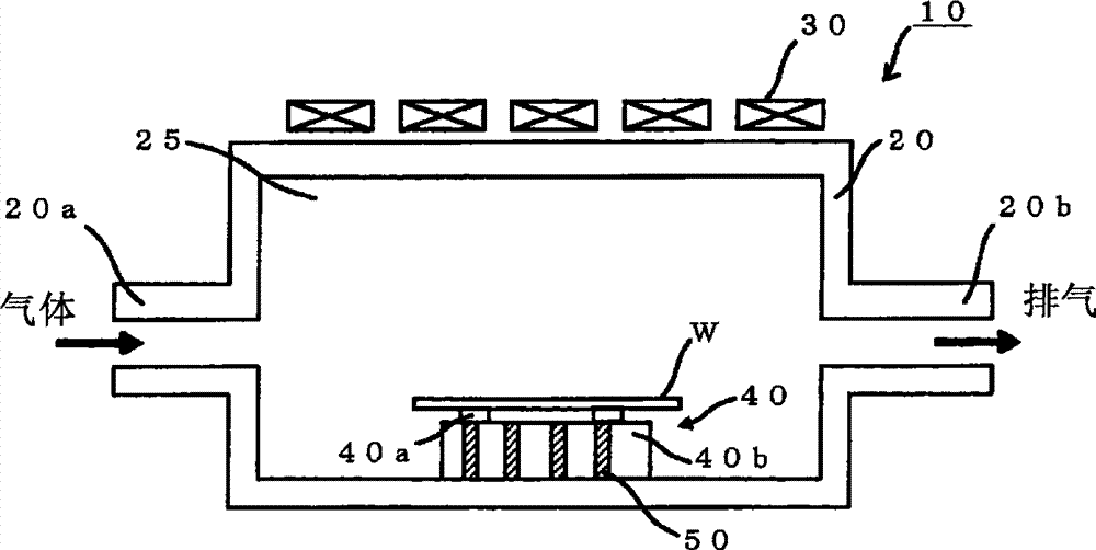
[0126] figure 1 It is a cross-sectional view schematically showing an example of an RTP device used in the method of manufacturing a silicon wafer of the present invention.
[0127] Such as figure 1 As shown, the RTP apparatus 10 used in the method of manufacturing a silicon wafer of the present invention includes: a reaction tube 20 having an atmospheric gas inlet 20a and an atmospheric gas discharge port 20b; The reaction space 25 in the reaction tube 20 supports the wafer support part 40 of the wafer W. The wafer support unit 40 includes an annular susceptor 40a that directly supports the wafer W, and a stage 40b that supports the susceptor 40a. The reaction tube 20 is made of, for example, quartz. The lamp 30 is constituted by, for example, a halogen lamp. The receptor 40a is made of silicon, for example. The stage 40b is made of quartz, for example.
[0128] in use as figure 1 When the shown RTP apparatus 10 performs rapid heating and rapid cooling heat treatment (...
Embodiment 1
[0176] The P-type, crystal plane orientation (001), solid dissolved oxygen concentration [Oi] was 1.2×10 produced by the CZ method. 18 atom / cm 3 (calculated value based on the conversion factor of Old ASTM), a single crystal silicon block with an impedance of 23-25Ω / cm.
[0177] At this time, the silicon wafer covered with the silicon nitride film was put into the nitrogen doping process, and the average crystal pulling speed was adjusted to 1.2mm / min. The crystal pulling rate V and the rate gradient G in the direction of the crystal axis at 1300° C. are controlled, thereby performing crystal pulling while controlling V / G.
[0178] Then, the obtained monocrystalline silicon ingot was cut into wafers with a wire saw, and subjected to beveling, polishing, etching, and grinding to produce a silicon wafer with a diameter of 300 mm polished on both sides.
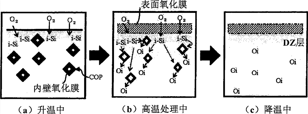
[0179] Then, several silicon wafers produced were sampled in the same group. The native defects on the device surface of th...
Embodiment 1-2
[0186] The P-type, crystal plane orientation (001), solid dissolved oxygen concentration [Oi] 1.0×10 was produced by the CZ method. 18 atom / cm 3 (calculated value based on the conversion factor of Old ASTM), impedance 28-30Ω / cm, and a silicon wafer with a diameter of 300 mm polished on both sides was produced by the same method as in Example 1-1.
[0187] Next, several silicon wafers were sampled in the same group. The native defects on the device surface of the sampled silicon wafer were observed by AFM (Atomic Force Microscopy). The maximum value of the size converted to the diameter of a sphere having the same volume as the observed native defect was determined. As a result, the maximum value of the COP measured in Example 1-2 was 100 nm.
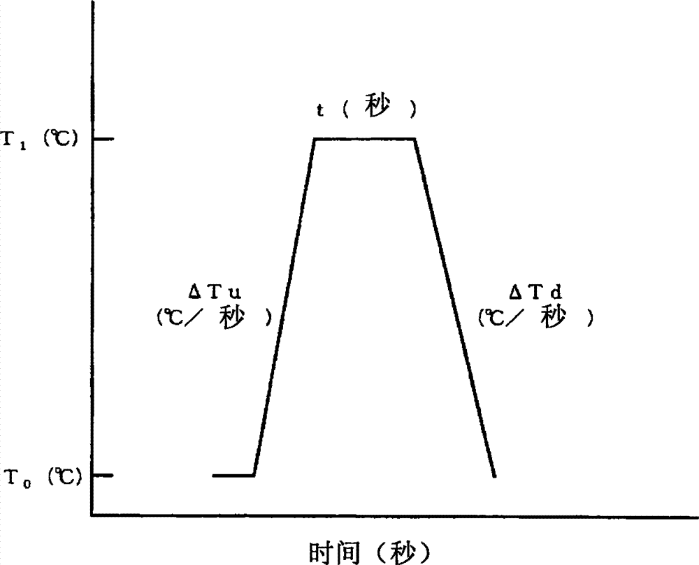
[0188] Second, use such as figure 1 The shown RTP device 10 performs rapid heating and rapid cooling heat treatment on the silicon wafer produced above. In embodiment 1-2, in such as figure 2 In the temperature program shown, the ...
PUM
| Property | Measurement | Unit |
|---|---|---|
| depth | aaaaa | aaaaa |
| diameter | aaaaa | aaaaa |
| depth | aaaaa | aaaaa |
Abstract
Description
Claims
Application Information