Light-sensing organic field-effect transistor and preparation method thereof

An organic field and transistor technology, which is applied in the field of light-sensing organic field-effect transistors and its preparation, can solve the problems of lack of applications of different aggregation states of high light-sensitive semiconductors, and achieve the effects of low cost, high response, and good application prospects

Inactive Publication Date: 2010-02-10
INST OF CHEM CHINESE ACAD OF SCI
View PDF0 Cites 11 Cited by
  • Summary
  • Abstract
  • Description
  • Claims
  • Application Information

AI Technical Summary

Problems solved by technology

However, the above research has not really reached the level comparable to that of amorphous silicon PTs in various important indicators. The reason is due to the lack of development of high photosensitive semiconductors and insufficient research on the application of different aggregation states in devices.

Method used


Image

  • Light-sensing organic field-effect transistor and preparation method thereof
  • Light-sensing organic field-effect transistor and preparation method thereof
  • Light-sensing organic field-effect transistor and preparation method thereof

Examples


Embodiment 1

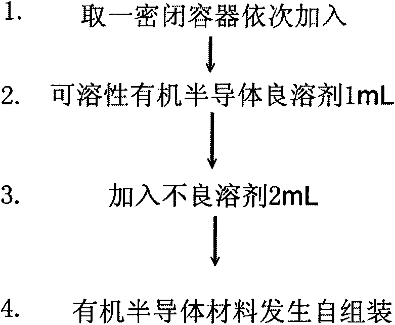
[0049] This embodiment prepares light-sensing organic field-effect transistor according to the following steps:

[0050] 1) The substrate layer used is a single crystal silicon wafer with a thickness of 400-500 microns, and the gate electrode is highly doped silicon (such as nitrogen or phosphorus, with a doping concentration of 1 to 9×10 per cubic meter. 20 ), the thickness of the gate electrode is about 400-500 microns;

[0051] 2) According to silicon thermal oxidation method (Wang Yongzhen, Gong Guoquan, Cui Jingzhong, Preparation and Application of Silicon Dioxide Thin Film, Vacuum and Low Temperature, 2003, 9, 228), an insulating layer was prepared on the gate electrode, and the material constituting the insulating layer was dioxide Silicon; wherein, the temperature of thermal oxidation is 900-1200°C, and the thickness of the insulating layer is 500 nanometers;

[0052] 3) The substrate deposited with an insulating layer obtained in step 2) is ultrasonically cleaned wit...

Embodiment 2

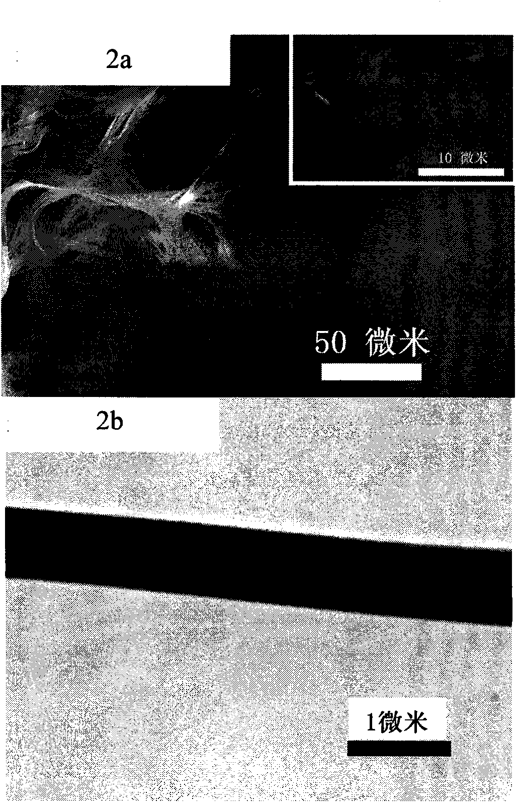
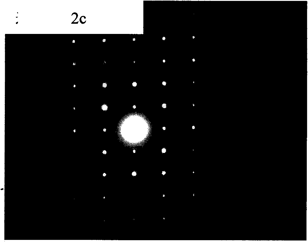
[0077] According to the same preparation method as in Example 1, only the good solvent in step 4) is changed to chloroform, and the poor solvent is methanol, and the photosensitive organic field effect is obtained under the same preparation conditions as in Example 1 above. Transistor, the morphology and device performance of the transistor are the same as those in Example 1.

Embodiment 3

[0079] According to the same preparation method as in Example 1, only the good solvent in step 4) was changed to toluene, and the poor solvent was methanol, and the light-sensing organic field effect transistor was obtained under the same preparation conditions as in Example 1 above, The morphology and device performance of the transistor are the same as those in Example 1.


PUM

PropertyMeasurementUnit
lengthaaaaaaaaaa
diameteraaaaaaaaaa
thicknessaaaaaaaaaa

Abstract

The invention discloses a light-sensing organic field-effect transistor and a preparation method thereof. The transistor comprises a substrate, a grid electrode arranged on the substrate and an insulating layer arranged on the grid electrode; the transistor further comprises a self-assembled monomolecular-modified layer and a source electrode, a drain electrode and at least one organic semiconductor compound single crystal wire positioned on the self-assembled monomolecular layer. The self-assembled monomolecular layer comprises materials of octadecyltrichlorosilane, octacyltrichlorosilane, phenyltrichlorosilane and the like; and the preferential organic semiconductor compound is 6-methyl-anthracene [2,3-b] benzo-[d] thiophene. The length of the organic semiconductor compound single crystal is 80-300 microns, and the diameter is 1-10 microns. The preparation method provided by the invention has simple prepration process and low cost, and the prepared organic field-effect transistor has very high response on a low-energy light source with the energy of 10-90 microwatts per square centimeter, high mobility, high photosensitivity and high ratio of light current to dark current.

Description

technical field [0001] The invention relates to the technical field of organic field effect transistor sensing, in particular to an optical sensing organic field effect transistor and a preparation method thereof. Background technique [0002] With the development of organic electronics, organic field-effect transistors (OFETs) have the unique advantages of light weight, easy flexibility and low cost, as well as wide application prospects in circuit driving and sensitive sensors. attract people's attention. Among numerous researches on OFETs, organic phototransistors (OPTs) with switching performance and light sensing function of OFETs are a very promising class of optoelectronic devices. The reason is that OPTs has its own unique advantages: the same photosensitive principle, but has a better signal amplification function; its structure is easier to integrate on a large scale than junction field effect transistors (Y.-Y.Noh , D.-Y.Kim, and K.Yase, J.Appl.Phys.2005, 98, 07...

Claims


Application Information

Patent Timeline
Patent Type & Authority Applications(China)
IPC IPC(8): H01L51/00H01L51/05H01L51/42H01L31/113H01L51/40H01L51/48C07F7/12C07D333/50
CPCY02E10/549Y02P70/50
Inventor 于贵郭云龙杜春燕蒋士冬狄重安闫寿科刘云圻
Owner INST OF CHEM CHINESE ACAD OF SCI
Why Eureka
Try Eureka