

Carrier-storing grooved gate IGBT with P-type floating layer
A carrier storage and floating layer technology, applied in the direction of electrical components, circuits, semiconductor devices, etc., can solve the problems of increased forward voltage drop and poor forward conduction characteristics of devices, so as to reduce forward voltage drop, Effect of improving forward conduction characteristics and increasing design margin
- Summary
- Abstract
- Description
- Claims
- Application Information
AI Technical Summary
Problems solved by technology
Method used
Image

Examples
Embodiment Construction
[0037] By adopting the novel carrier storage trench gate IGBT structure with P-type floating layer of the present invention, lower on-voltage drop, large forward bias safe operating area (FBSOA) and short circuit safe operating area (SCSOA) can be obtained, and The breakdown voltage can be further improved, the manufacture is simple, and the design margin is large. With the development of semiconductor technology, more power devices with low voltage drop and high reliability can be produced by using the present invention.
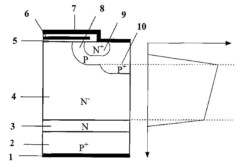
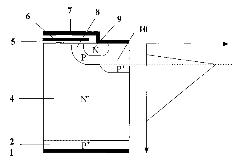
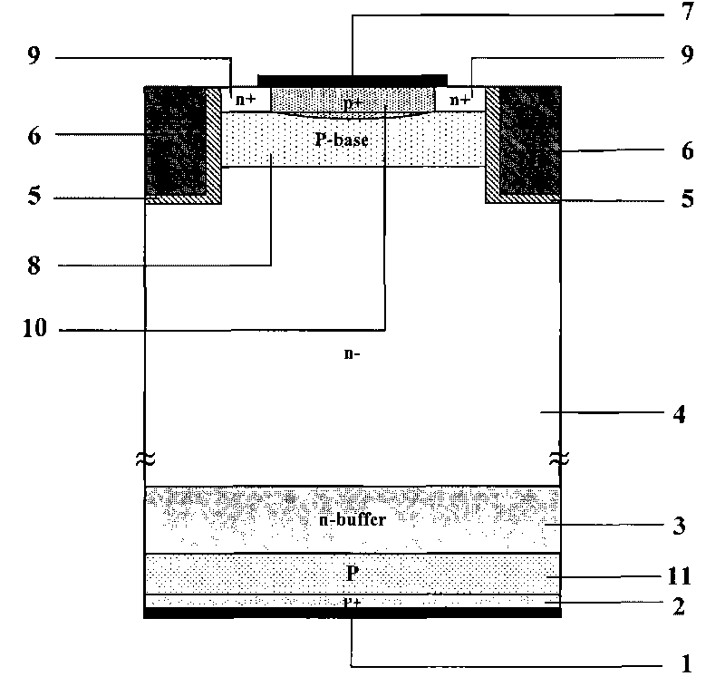
[0038] A carrier storage trench gate IGBT with a P-type floating layer, such as Image 6 shown, each cell includes collector 1, P + Collector region 2, P-type collector region 11, N-type buffer layer 3, N - Base region 4, P-type floating layer 13, gate oxide layer 5, polysilicon gate 6, emitter 7, N + Source Region 9, P + Body region 8 , N-type carrier storage layer 12 . The gate oxide layer 5 and the polysilicon gate 6 form a trench deletion structure...
PUM
 Abstract
Description
Claims
Application Information