GaN-based LED chip extending and growing method for reducing dislocation defects

A technology of LED chips and epitaxial growth, which is applied in the field of optoelectronics, can solve problems such as increased defects, and achieve the effect of improving crystal quality, high quality, and performance

Inactive Publication Date: 2010-05-05
Shandong Huaguang Optoelectronics Co. Ltd.
View PDF1 Cites 23 Cited by
  • Summary
  • Abstract
  • Description
  • Claims
  • Application Information

AI Technical Summary

Problems solved by technology

This document uses an in-situ SiN (silicon nitride) mask to reduce the defects in GaN, but from the experience of practical application, the SiH introduced when making the in-situ SiN mask 4 (Silane) has a strong corrosion effect on GaN at the beginning, causing many holes on the surface of GaN, resulting in more defects in GaN materials

Method used


Image

  • GaN-based LED chip extending and growing method for reducing dislocation defects
  • GaN-based LED chip extending and growing method for reducing dislocation defects
  • GaN-based LED chip extending and growing method for reducing dislocation defects

Examples


Embodiment 1

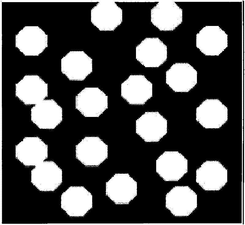
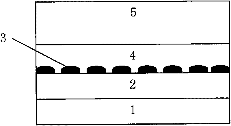
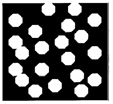
[0018] First put the sapphire substrate 1 into the reaction chamber of the MOCVD (metal organic chemical vapor deposition) growth furnace, and the reaction chamber is in the H 2 Heat the sapphire substrate to 1100°C for 15 minutes in the atmosphere, then lower the temperature to 535°C for 10 minutes, and grow a low-temperature GaN buffer layer with a thickness of 30nm on the substrate. The source material used is trimethylgallium and NH 3 . Then the temperature of the reaction chamber is raised to 1060° C. within 8 minutes. During this process, the low-temperature GaN buffer layer is thermally annealed to recrystallize it, and a high-temperature non-doped GaN layer 2 with a thickness of 100nm-2000nm is grown at this temperature. Then pass Cp alone in the reaction chamber 2 Mg (magnesocene) source and NH 3 , the two react to form a MgN composite 3, uniformly covering the high-temperature GaN layer 2, and passing through the CP 2 The Mg time is 3 minutes, and the thickness o...

Embodiment 2

[0021] Put the SiC substrate 1 into the reaction chamber of the MOCVD growth furnace first, and the reaction chamber is in the H 2 Heat the substrate to 1100°C for 15 minutes in the atmosphere, then lower the temperature to 1000°C-1100°C in 3 minutes, and grow a high-temperature AlxGa1-xN buffer layer with a thickness of 10nm-200nm on the substrate, where 03 and CP 2 Mg, forming a MgN mask. A 1 um thick high temperature non-doped GaN layer 4 is then grown subsequently on the MgN cap. Finally, other epitaxial materials 5 for epitaxial GaN-based LED chips include Si-doped n-type GaN, InGaN / GaN multiple quantum wells, and Mg-doped GaN.

Embodiment 3

[0023] First put the Si substrate 1 into the reaction chamber of the MOCVD growth furnace, and the reaction chamber is in the H 2Heat up the Si substrate to 1100°C for 15 minutes in the atmosphere, then lower the temperature to 1000°C for 5 minutes, and grow a 10nm-30nm high-temperature AlxGa1-xN buffer layer on the substrate, where 03 and CP 2 Mg, forming a magnesium nitride mask 3 . A 1 um thick high temperature non-doped GaN layer 4 is then grown subsequently on the MgN cap. Finally, other epitaxial materials 5 for epitaxial GaN-based LED chips include Si-doped n-type GaN, InGaN / GaN multiple quantum wells, and Mg-doped GaN.


PUM


Abstract

The invention provides a GaN-based LED chip extending and growing method for reducing dislocation defects, comprising the following steps of: (1) firstly, growing a low-temperature GaN buffer layer or AlxGal-xN buffer layer on a substrate, and then growing a high-temperature undoped GaN layer on the buffer layer; (2) regulating the growing temperature in a reaction chamber to 600DEG C to 1100 DEG C ,and then independently introducing CP2Mg and NH3 into the reaction chamber, reacting the CP2Mg with the NH3 to form MgN on the high-temperature undoped GaN layer made in step (1), wherein the sizes and density of the holes are controlled through the time for introducing the CP2Mg; (3) continuously growing other extending materials of a GaN-based LED chip according to the normal method. The invention adopts the MgN to make a nano masking figure in situ to reduce the dislocation defects in a GaN-based material. Compared with SiN masking, the invention has no corrosion on the GaN material when making the MgN masking, and therefore, the GaN having no a masking position can not introduce more defects, and the GaN material with higher quality can be acquired.

Description

technical field [0001] The invention relates to a GaN-based LED chip epitaxial growth method for reducing dislocation defects, and belongs to the field of optoelectronic technology. Background technique [0002] Group III nitrides represented by GaN (AlN, GaN, InN, AlGaInN) have excellent photoelectric properties, so they are widely used in blue light, green light, ultraviolet light-emitting diodes (LEDs) and high-frequency, high-temperature, high-power electronic devices. application. Due to the lack of lattice-matched substrates, III-nitrides are heterogeneously epitaxy on other materials. Commonly used substrates include sapphire, silicon carbide, silicon, gallium arsenide, zinc oxide, etc., and commonly used epitaxy methods include metal organics Chemical vapor deposition (MOCVD), molecular beam epitaxy (MBE) and hydride vapor phase epitaxy (HVPE), etc. Due to the large lattice mismatch and thermal mismatch with the substrate, even after the low-temperature GaN buffer ...

Claims


Application Information

Patent Timeline
Patent Type & Authority Applications(China)
IPC IPC(8): H01L33/00H01L33/16H01L33/06
Inventor 朱学亮吴德华曲爽吴亭李树强徐现刚任忠祥
Owner Shandong Huaguang Optoelectronics Co. Ltd.
Why Eureka
Try Eureka