Thyristor core manufacturing process

A manufacturing process and thyristor technology, applied in semiconductor/solid-state device manufacturing, electrical components, circuits, etc., can solve the problems of low die withstand voltage level, poor die mechanical properties, low reliability, etc., to ensure dynamic characteristics, Simplified die manufacturing process, easy removal effect

Inactive Publication Date: 2010-06-23
ZHEJIANG SIFANG ELECTRONICS
View PDF0 Cites 15 Cited by
  • Summary
  • Abstract
  • Description
  • Claims
  • Application Information

AI Technical Summary

Problems solved by technology

[0002] The traditional manufacturing process of the traditional welded thyristor core is to use the "double diffusion-nickel plating method", by chemically plating the surface of a single crystal silicon wafer that has undergone boron diffusion (primary diffusion) and phosphorus diffusion (secondary diffusion), To make it possible to achieve weldable process characteristics, and then through the lead enamel process, the single crystal silicon wafer and the molybdenum sheet that has also been electroless nickel plated are welded together. After conventional grinding, surface corrosion and other processes, a weldable Welded thyristor cores are only suitable for soldered thyristor packaging and manufacturing. The advantage of this method is that the cathode electrode can be drawn out smoothly after the surface of the core part is a single crystal silicon wafer after electroless nickel plating. It makes the die have weldable process characteristics, simplifies the packaging process, and improves the production efficiency of the welded thyristor die; but the disadvantage is that the repeatability and consistency of the dynamic parameters of the thyristor die made by this process are relatively low. Poor, poor high temperature characteristics (welded thyristor core according to the electrical industry standard JB / T8950.1-1999, the working junction temperature of the thyristor with a current less than 100A under high temperature state is usually 115 ℃), the produced core voltage rating low (usually the soldered core withstand voltage level can only reach 2000V), the grade pass rate is not high and other shortcomings; and because this process adopts the traditional manual lead filling, the single crystal silicon wafer and the electroless nickel plated The molybdenum sheet (in the traditional process, the molybdenum sheet needs to be electroless nickel-plated before the lead-coating treatment) is soldered to form the die by the lead-coating process, and there are many interferences from human factors, which leads to low manufacturing efficiency of the die, and it is difficult to guarantee the quality of the finished product; More importantly, the current solder usually uses lead and tin as the raw and auxiliary materials, resulting in the lead content of the finished tube core being too high, far exceeding the requirements for lead content in the EU ROHS directive (the lead content requirements for products in the ROHS directive: the highest shall not exceed 1000mg / kg), seriously affecting the export of welded thyristors and power modules manufactured by traditional techniques in China
Although domestic manufacturers have used silver-tin and other lead-free solder instead of lead-tin solder to solder the die, the melting point of silver-tin and other lead-free solder is much higher than that of lead-tin solder (the melting point of lead-tin solder is about 183°C, the melting point of lead-free solder such as silver tin is at least 217°C), the lead-free alloy solder has poor wetting ability, and cannot be automatically aligned. The mechanical properties are poor, the solder joints are very brittle, they are easy to fall off after collision, and the reliability is low. At the same time, because the soldering process is still used, the high temperature characteristics and withstand voltage level of the die cannot be improved and improved.

Method used


Image

  • Thyristor core manufacturing process
  • Thyristor core manufacturing process

Examples


Embodiment 1

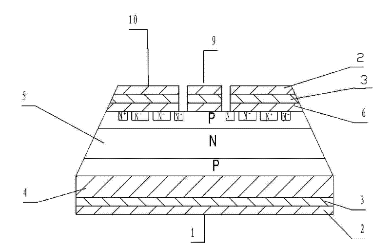
[0026] The specific manufacturing process and steps of the present invention are as follows, wherein boron diffusion, oxidation, primary photolithography, phosphorous diffusion, secondary photolithography, surface corrosion, and angle grinding are all conventional thyristor tube core manufacturing methods.

[0027] 1. Boron diffusion: adopt the conventional coating diffusion method, use ultra-pure diboron trioxide and pure aluminum nitrate to configure the impurity source, apply the impurity source on the surface of the prepared single crystal silicon wafer, and place it in a diffusion furnace at 1200°C. Constant temperature for 25h, diffusion in the atmosphere, so that borosilicate glass body is formed on the surface of the silicon wafer, forming a P-N-P structure (that is, forming j1 junction and j2 junction), and then polishing;

[0028] 2. Oxidation: Clean the surface of the boron-diffused silicon wafer with a cleaning solution, dehydrate it for use, and then put the cleane...

Embodiment 2

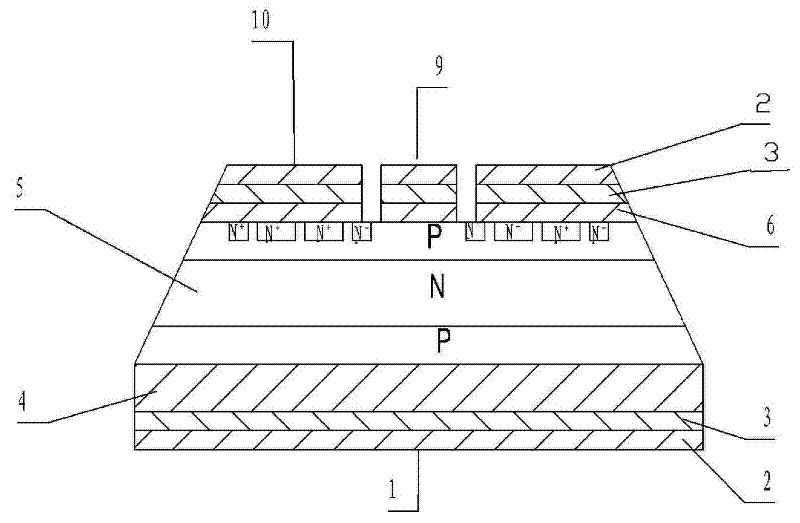
[0041] Concrete manufacturing process and steps of the present invention are as follows:

[0042] 1. Boron diffusion: adopt the conventional coating diffusion method, use ultra-pure diboron trioxide and pure aluminum nitrate to configure the impurity source, apply the impurity source on the surface of the prepared single crystal silicon wafer, and place it in a diffusion furnace at 1400°C. Constant temperature for 40h, diffusion in the atmosphere, so that borosilicate glass body is formed on the surface of the silicon wafer, forming a P-N-P structure (that is, forming j1 junction and j2 junction), and then polishing;

[0043] 2. Oxidation: Clean the surface of the boron-diffused silicon wafer with a cleaning solution, dehydrate it for use, and then put the cleaned and dehydrated silicon wafer into a diffusion furnace for oxidation treatment, in which dry oxygen for 60 minutes, Wet oxygen for 150 minutes, dry oxygen for 60 minutes, wet oxygen for 130 minutes, dry oxygen for 100...


PUM

PropertyMeasurementUnit
thicknessaaaaaaaaaa

Abstract

The invention discloses a thyristor core manufacturing process. The manufacturing process is characterized in that the manufacturing process includes the following steps: 1) boron diffusion; 2) oxidization; 3) primary photoetching; 4) phosphorus diffusion; 5) sintering; 6) evaporation; 7) alloying; 8) secondary photoetching; 9) surface treatment-nickeling; 10) surface treatment-silvering; 11) tertiary photoetching; 12) angle grinding; 13) surface corrosion. Primary diffusion-oxidization-photoetching-secondary diffusion are carried out on an original N-type silicon slice so as to form a four-layer (P-N-P-N) structure; sintering and bonding are carried out under the vacuum condition and high temperature; high-purity aluminum is gasified on the surface of a mono-crystalline silicon slice by an electron beam under high temperature so as to form an effective protective film; finally, nickeling and silvering treatments are respectively carried out on a surface layer of a sintered and film-coated thyristor core, and an anode and a cathode which can be welded are led out at the two ends of the thyristor core, so as to prepare the entire thyristor core suitable for both welding encapsulation and pressure-welding encapsulation at the same time as removing a traditional lead evading technology.

Description

technical field [0001] The invention relates to a semiconductor device, in particular to a manufacturing process of a thyristor. Background technique [0002] The traditional manufacturing process of the traditional welded thyristor core is to use the "double diffusion-nickel plating method", by chemically plating the surface of a single crystal silicon wafer that has undergone boron diffusion (primary diffusion) and phosphorus diffusion (secondary diffusion), To make it possible to achieve weldable process characteristics, and then through the lead enamel process, the single crystal silicon wafer and the molybdenum sheet that has also been electroless nickel plated are welded together. After conventional grinding, surface corrosion and other processes, a weldable Welded thyristor cores are only suitable for soldered thyristor packaging and manufacturing. The advantage of this method is that the cathode electrode can be drawn out smoothly after the surface of the core part i...

Claims


Application Information

Patent Timeline
Patent Type & Authority Applications(China)
IPC IPC(8): H01L21/332H01L21/60
Inventor 何加利
Owner ZHEJIANG SIFANG ELECTRONICS
Why Eureka
Try Eureka