Production method of basement for enhancing raman scattering of molecule
A Raman scattering and manufacturing method technology, applied in the micro-nano field, can solve the problems of poor repeatability and stability, low detection sensitivity, and low Raman scattering efficiency of molecules to be measured, so as to improve molecular Raman scattering and enrichment effect of ability
- Summary
- Abstract
- Description
- Claims
- Application Information
AI Technical Summary
Problems solved by technology
Method used
Image
Examples
Embodiment 1
[0028] In TNT gas trace detection, the preparation method of the present invention is:
[0029] (1) Choose K9 glass as the base substrate, put it into the washing solution made of concentrated sulfuric acid with a concentration of 90% to 98% and hydrogen peroxide H2SO4: 30% H2O22 to 4:1 and heat it to 80°C to 120°C for 30 to 60 minutes , to remove impurities, then rinse repeatedly, then put ammonia, hydrogen peroxide and water into the solution NH3:H2O2:H2O / 1:1:5 for ultrasonic treatment for 20 to 60 minutes, then take out the substrate for repeated washing, save, and ready for use;
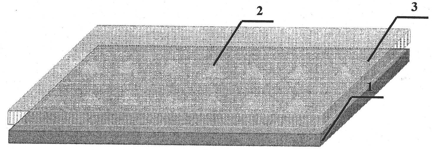
[0030] (2) Design a hexagonal triangular metal nanostructure, the metal structure material is gold, the characteristic size is 100nm, the period is 500nm, and the thickness is 10nm. The plasmon resonance frequency of this structure is about 420nm. Fabricating a metal micro-nano structure 2 on the base substrate 1 by nanoimprinting method;
[0031] (3) metallizing the micro-nano structure by vap...
Embodiment 2
[0036] In sucrose solution probing, substrate fabrication is achieved by the following steps
[0037] (1) Silicon is selected as the substrate, cleaned and treated for hydrophilicity.
[0038] (2) A nanostructure with a triangular distribution, a characteristic size of 50nm, and a period of 300nm is produced on the surface of the substrate by self-assembly of nanospheres.
[0039] (3) Metallize the nanostructure by magnetron sputtering, first sputter a layer of metallic silver, and then change the target to sputter a layer of metallic gold to obtain a double-layer metal with 50nm gold and 20nm thick silver Substrates for nanometallic structures.
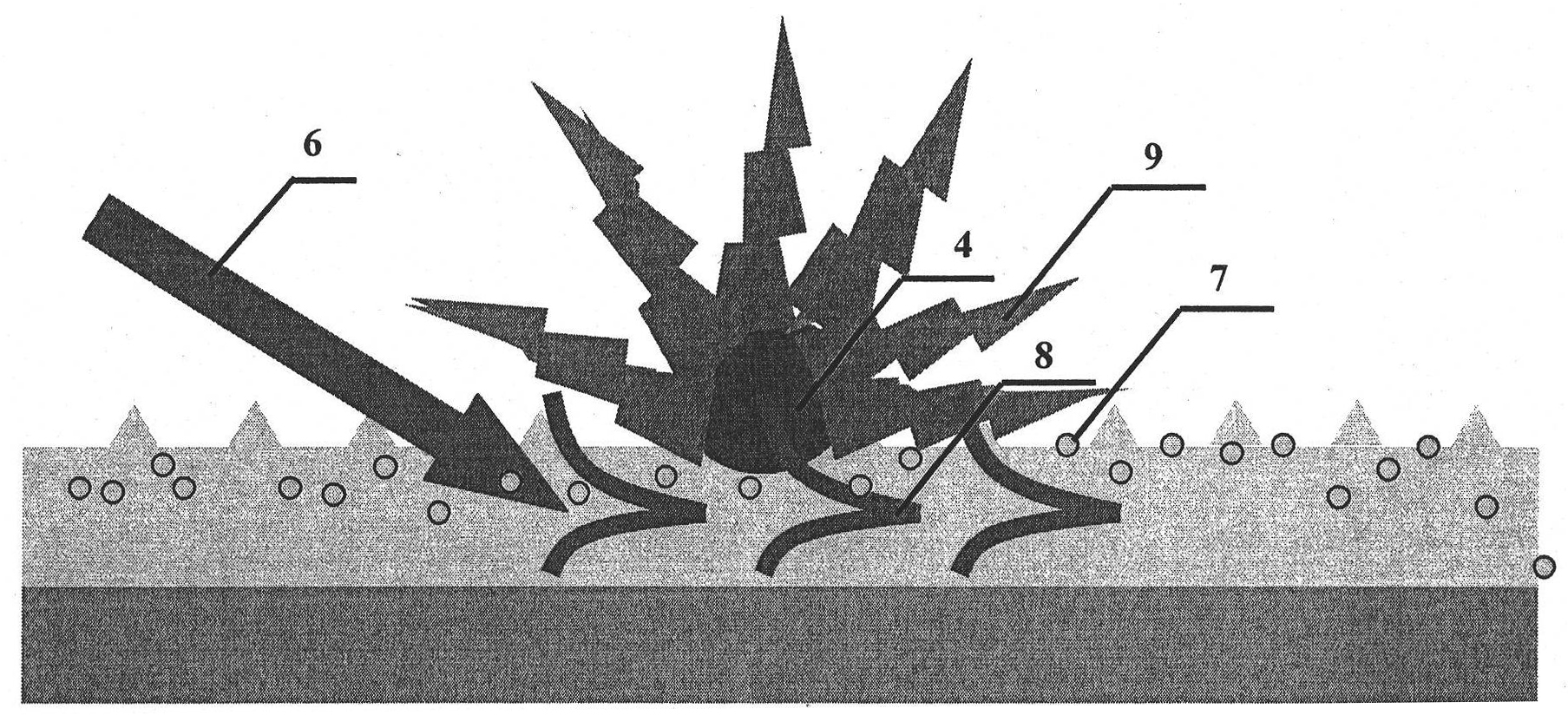
[0040] (4) If the substrate is directly placed in the solution to be tested for detection, the adsorption of the substrate to be tested is as follows: Figure 4 shown. Add a layer of molecular biofilm 3 to the surface of the substrate and activate it: prepare a 1 mM solution of octanethiol (1-octanethiol, 1-OT) and sulfhydryl-cont...
Embodiment 3
[0043] In the detection of charcoal distance virus powder, the fabrication of the substrate is achieved through the following steps
[0044](1) select germanium as the substrate material, clean and do hydrophilic treatment;
[0045] (2) Nanoimprinting is used to produce a nanostructure layer with a characteristic size of 800nm, a period of 3μm, and a quadrilateral arrangement on the surface of the substrate;
[0046] (3) Metallize the micro-nano structure layer, first sputter a layer of metal gold, then change the target and sputter a layer of metal silver to obtain a nano-metal structure with a double-layer metal of 300nm gold and 100nm thick silver end;
[0047] (4) modifying the surface of the substrate obtained in step (3) to obtain a surface decoration layer, preparing an adsorption film to improve the ability of the substrate to enrich the molecules to be measured, and activating the substrate;
[0048] (5) Adding molecules to be measured to the substrate with the surf...
PUM
| Property | Measurement | Unit |
|---|---|---|
| size | aaaaa | aaaaa |
| thickness | aaaaa | aaaaa |
| thickness | aaaaa | aaaaa |
Abstract
Description
Claims
Application Information


