

Processing method of differential type high-precision accelerometer
An accelerometer and processing method technology, applied in the direction of velocity/acceleration/shock measurement, acceleration measurement, metal processing equipment, etc. Reduce the effect of stress, reduce the effect of process temperature
- Summary
- Abstract
- Description
- Claims
- Application Information
AI Technical Summary
Problems solved by technology
Method used
Image

Examples
Embodiment Construction
[0033] In order to make the above objects, features and advantages of the present invention more comprehensible, the present invention will be further described in detail below in conjunction with the accompanying drawings and specific embodiments.
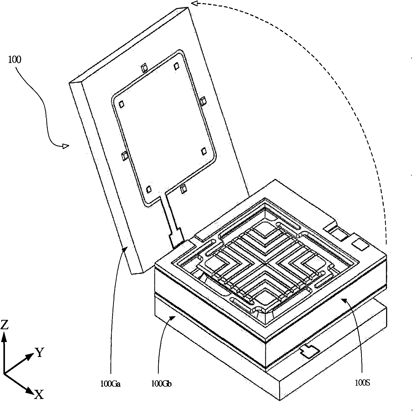
[0034] Such as Figure 1~3B It is a structural diagram of a micromachined differential capacitance accelerometer with a symmetrical structure, and a method for preparing the movable silicon structural component (beam-mass structure) of the accelerometer in the present invention. figure 1 Shown is a schematic structural view of the accelerometer (glass electrode cover plan) of the present invention. Such as figure 1 As shown, the accelerometer 100 has a glass upper electrode cover 100Ga, a glass lower electrode cover 100Gb, and a movable silicon structure assembly 100S.
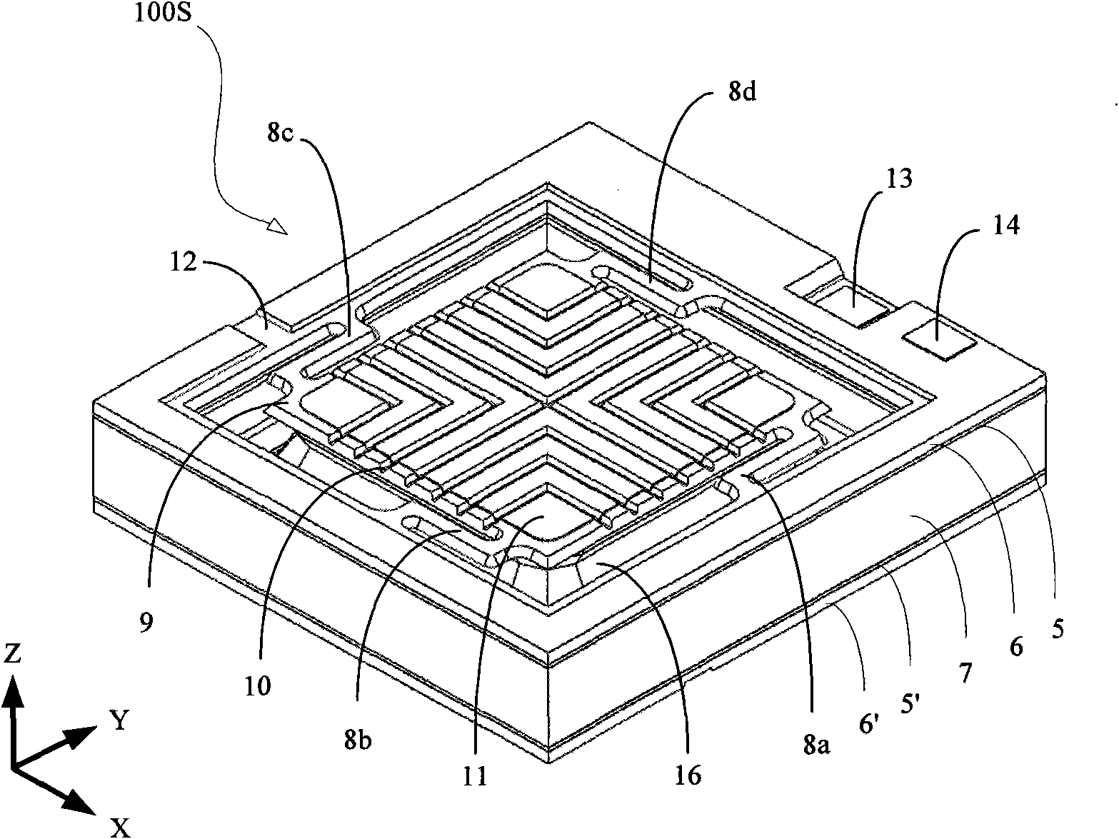
[0035] figure 2 Shown is a schematic structural diagram of the movable silicon structural component 100S, wherein 8a, 8b, 8c, and 8d are elastic support beams...
PUM
 Abstract
Description
Claims
Application Information