Nano crystal Cr2N/amorphous WC superhard film with superlattice structure and preparation method thereof
A superlattice and nanocrystalline technology, applied in the field of Cr2N/WC superlattice film, can solve problems such as the difficulty of superhard Cr-N film, achieve the effect of improving high temperature performance, expanding the application range, and improving the bonding strength
- Summary
- Abstract
- Description
- Claims
- Application Information
AI Technical Summary
Problems solved by technology
Method used
Image
Examples
Embodiment 1
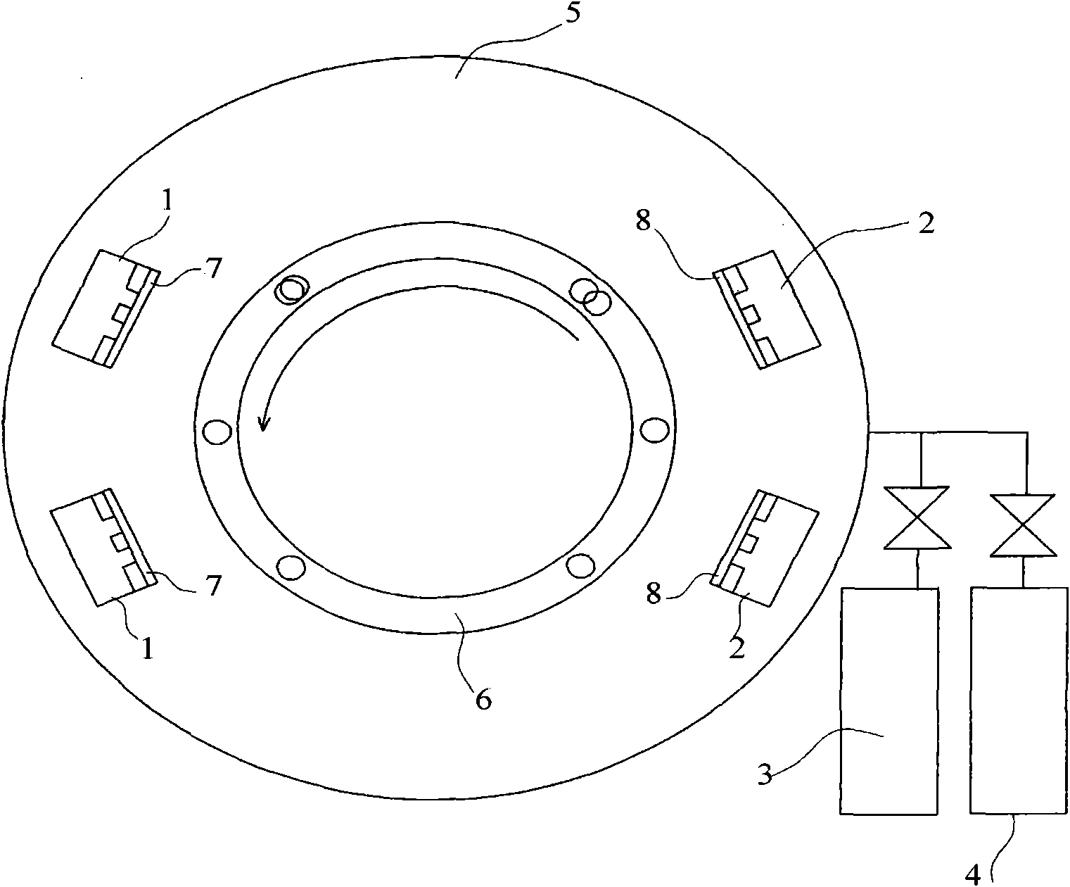
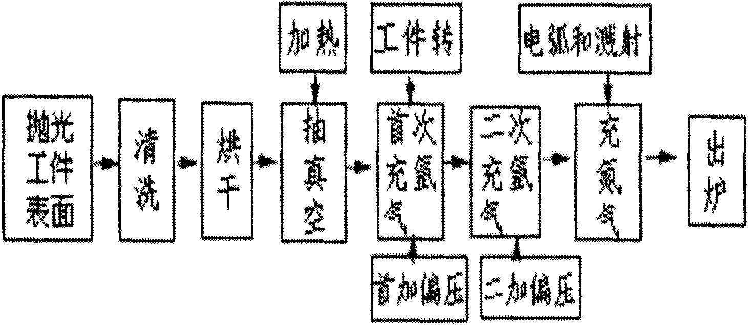
[0031] Embodiment 1: as figure 1 and figure 2 As shown, a pair of intermediate frequency DC magnetron sputtering sources 7 are adjacently installed on one side of the vacuum chamber and in front of the intermediate frequency DC magnetron device 1, and two arc sources 8 are installed on the opposite side, and are located on the respective arc Generator 2, N 2 Bottle 3 and Ar bottle 4 can be adjusted to pass into the vacuum chamber 5; choose Si (001) as the base material (workpiece 001), and the size is 1×30×40mm 3 , after polishing, ultrasonically clean with acetone and alcohol for 10 minutes each, and install on the workpiece turret 6 in the vacuum chamber 5 after drying. The vacuum degree of the vacuum chamber 5 is 3.5×10 -3 Pa, the heating temperature of workpiece 001 is 320°C, and the workpiece 001 rotates 10 rpm; the flow rate of Ar gas is 20SCCM, the bias voltage is 600V, and the surface of the workpiece is bombarded and cleaned with Ar ions for 10min; the bias voltag...
Embodiment 2
[0035] Embodiment 2: choose Si (001) as base material (work piece 002), size is 1 * 30 * 40mm 3 , after polishing, ultrasonically clean with acetone and alcohol for 10 minutes each, and install on the workpiece turret 6 in the vacuum chamber 5 after drying. The vacuum degree of the vacuum chamber 5 is 3.5×10 -3 Pa, the heating temperature of the workpiece 001 is 320°C, and the workpiece 001 rotates 10 rpm; the flow rate of the Ar gas is 20SCCM, the bias voltage is 600V, and the surface of the workpiece is bombarded and cleaned with Ar ions for 10min; the bias voltage is reduced to 500V, The starting arc source and the intermediate frequency DC magnetron sputtering source were used to deposit Cr and WC multi-component amorphous transition layers, respectively, and worked for 10 minutes; filled with N 2 Gas flow is 40SCCM for depositing Cr 2 N and WC layers, work for 60 minutes; when the vacuum chamber 5 is cooled to room temperature, open the furnace door and take out the wor...
Embodiment 3
[0039] Embodiment 3: In order to detect the binding force between the film layer and the substrate under the same process conditions as in Example 1, choose die steel SKD11 as the substrate material (workpiece 003), with a size of 5 × 30 × 50mm 3 , after polishing, ultrasonically clean with acetone and alcohol for 10 minutes each, and install on the workpiece turret 6 in the vacuum chamber 5 after drying. The vacuum degree of the vacuum chamber 5 is 3.5×10 -3 Pa, the heating temperature of workpiece 001 is 320°C, and the workpiece 001 rotates 10 rpm; the flow rate of Ar gas is 20SCCM, the bias voltage is 600V, and the surface of the workpiece is bombarded and cleaned with Ar ions for 10min; the bias voltage is reduced to 400V, The starting arc source and the DC magnetron sputtering source were used to deposit Cr and WC multivariate amorphous transition layers respectively, and worked for 10 minutes; filled with N 2 Gas flow is 40SCCM for depositing Cr 2 N and WC layers, work...
PUM
| Property | Measurement | Unit |
|---|---|---|
| thickness | aaaaa | aaaaa |
| thickness | aaaaa | aaaaa |
| thickness | aaaaa | aaaaa |
Abstract
Description
Claims
Application Information


