Superlattice multilayer film and preparation method thereof

A multi-layer film and superlattice technology, used in coatings, layered products, nanostructure manufacturing, etc., can solve problems such as low hardness and limitations, and achieve the effect of improving bonding strength, improving stress distribution, and expanding application scope.

Inactive Publication Date: 2011-01-12
ANHUI DUOJINTUCENG TECH CO LTD
View PDF3 Cites 6 Cited by
  • Summary
  • Abstract
  • Description
  • Claims
  • Application Information

AI Technical Summary

Problems solved by technology

Found through literature search to prior art, Y.Liu etc. are in " TribologyInternational " (the tribological evaluation of WC / DLC solid lubricating film in vacuum) 2006 volume 39 pages 1584, this technology utilizes magnetron sputtering and ion etching The WC / DLC multilayer film is prepared systematically, so the WC phase is introduced. Although the thermal stability of the DLC film is increased on the basis of an extremely low friction coefficient, the hardness of the film is low, only 11GPa. Therefore, this type of coating The application of high-speed cutting tools for high-speed steel is greatly restricted

Method used


Image

  • Superlattice multilayer film and preparation method thereof
  • Superlattice multilayer film and preparation method thereof
  • Superlattice multilayer film and preparation method thereof

Examples


Embodiment 1

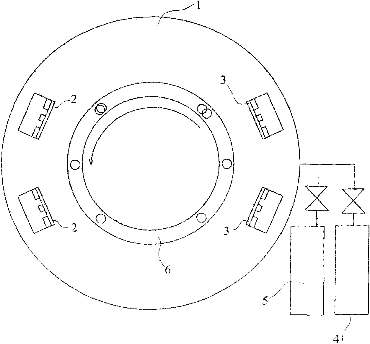
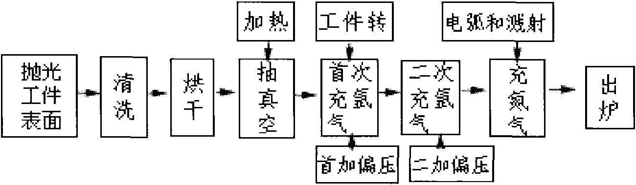
[0036] Such as figure 1 , figure 2 As shown, the present embodiment comprises the following steps: (1) one side in the vacuum chamber 1 is provided with a pair of intermediate frequency DC magnetron sputtering sources 2, and the other side is relatively provided with a pair of arc sources 3; N 2 Gas 4 and Ar gas 5 are connected to the vacuum chamber 1, and Si(001) is selected as the workpiece, and the size of the workpiece is 1×30×40mm 3 ;

[0037] (2) After polishing treatment, use acetone and alcohol to ultrasonically clean each for 10 minutes, and then install it on the turntable 6 in the vacuum chamber 1 after drying. The vacuum degree of the vacuum chamber 1 is 3.5×10 -3 Pa, the workpiece heating temperature is 320°C, and the workpiece rotates 10 revolutions / min;

[0038] (3) Pass Ar gas 5 into the vacuum chamber 1, the flow rate of the Ar gas 5 is 20SCCM, and the bias voltage is 600V, and the surface of the workpiece is bombarded and cleaned with Ar ions for 10 minut...

Embodiment 2

[0050] In this embodiment: Step (3) feeds Ar gas 5 into vacuum chamber 1, the flow rate of feeding Ar gas 5 is 20 SCCM, and the bias voltage is 600V, and Ar ion bombardment cleaning is carried out on the surface of the workpiece for 10 minutes to remove residual residues on the surface of the workpiece. After removing the adsorbates and oxides, reduce the bias voltage to 400V. Other implementation conditions are identical with embodiment 1.

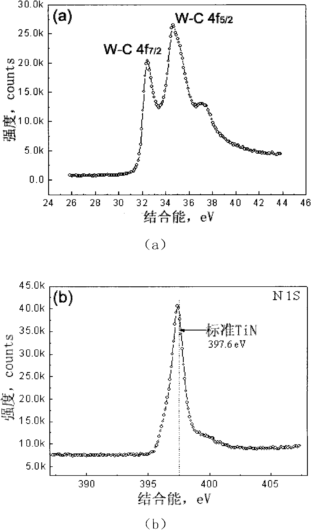
[0051] Such as Figure 5 As shown, by HRTEM detection and analysis, the modulation period of the superlattice obtained in this embodiment is 5nm, and the thicknesses of TiN and WC monolayers are about 4nm and 1nm respectively.

[0052] The total thickness of the superlattice multilayer film in this embodiment is 2.5 µm.

[0053] Such as Figure 7 As shown, the hardness of the superlattice multilayer film is detected by the nanoindentation method, the maximum load is 40mN, and the hardness value of the film layer is 52±2GPa.

[0054] S...

Embodiment 3

[0057] In the present embodiment: step (5) adds N to the vacuum chamber 1 2 Gas 4, add N 2 The flow rate of the gas 4 is 20 SCCM, and it works for 60 minutes to deposit and form the TiN nanocrystalline phase layer 7 and the WC amorphous phase layer. When the vacuum chamber 1 is cooled to room temperature, open the furnace door and take out the workpiece. Other implementation conditions are identical with embodiment 1.

[0058] Such as Figure 6 As shown, by HRTEM detection and analysis, the modulation period of the superlattice obtained in this embodiment is 3nm.

[0059] The total thickness of the superlattice multilayer film in this embodiment is 2.5 µm.

[0060] Such as Figure 7 As shown, the hardness of the superlattice multilayer film is detected by the nanoindentation method, the maximum load is 40mN, and the hardness value of the film layer is 44±2GPa.

[0061] Such as Figure 8 As shown, the hardness value and elastic modulus of the superlattice multilayer film ...


PUM

PropertyMeasurementUnit
Thicknessaaaaaaaaaa
Hardness valueaaaaaaaaaa
Fracture toughness valueaaaaaaaaaa

Abstract

The invention discloses a superlattice multilayer film and a preparation method thereof. The superlattice multilayer film comprises nanocrystal phase layers, an amorphous transition layer and amorphous phase layers, wherein the nanocrystal phase layers and the amorphous phase layers are alternately deposited on the amorphous transition layer. The preparation method comprises the following steps: arranging a magnetron sputtering source at one side of a vacuum chamber, and arranging an electric arc source at the other side; placing a polished and cleaned workpiece into the vacuum chamber, and setting process parameters; introducing Ar gas into the vacuum chamber, biasing to carry out Ar ion bombardment cleaning on the surface of the workpiece, and decreasing the bias; starting the electric arc source and the magnetron sputtering source, and depositing for certain time to generate a Ti / WC amorphous transition layer; and inflating N2 gas into the vacuum chamber for a certain time, and depositing to generate a TiN nanocrystal phase layer and WC amorphous phase layers. The obtained product is compact and uniform, and the bonding strength is improved. The invention realizes the superhardness effect and the high tenacity of the Ti / N-based film, and the amorphous WC layers in the superlattice multilayer structure also greatly improve the corrosion resistance and the oxidation resistance of the superlattice multilayer structure.

Description

technical field [0001] The invention relates to a coating film for workpiece surface treatment and a preparation method thereof, in particular to a superlattice multilayer film and a preparation method thereof. Background technique [0002] Transition metal nitride films are widely used as surface modifications for cutting and forming tools due to their advantages in hardness and wear resistance. The film layer has the following characteristics: good bonding force, sufficient thickness, appropriate mechanical properties (strength and hardness), thermal disturbance resistance and high temperature stability. Titanium nitride film has been widely used. It has the advantages of high hardness, good toughness, and thicker film layer. At the same time, it also has fine grain structure and strong bonding force, and has more practical value. [0003] With the advancement of modern plastic processing technology and the rapid development of aviation, aerospace, and automobile industri...

Claims


Application Information

Patent Timeline
IPC IPC(8): B32B9/00B82B1/00B82B3/00C23C14/35C23C14/32C23C14/06C23C14/14
Inventor 张世宏黄仲福方炜赵小燕
Owner ANHUI DUOJINTUCENG TECH CO LTD
Why Eureka
Try Eureka