Bulk silicon etching and gold silicon bonding combined process method

A composite process and bonding technology, applied in metal material coating process, process for producing decorative surface effects, decorative arts, etc., can solve the problems of redundancy and many process flows.

Active Publication Date: 2010-12-15
UNIV OF ELECTRONICS SCI & TECH OF CHINA
View PDF2 Cites 13 Cited by
  • Summary
  • Abstract
  • Description
  • Claims
  • Application Information

AI Technical Summary

Problems solved by technology

Therefore, the mask materials and bonding materials used in the process are different, and there are disadvantages of many and redundant processes

Method used


Image

  • Bulk silicon etching and gold silicon bonding combined process method
  • Bulk silicon etching and gold silicon bonding combined process method
  • Bulk silicon etching and gold silicon bonding combined process method

Examples


Embodiment 1

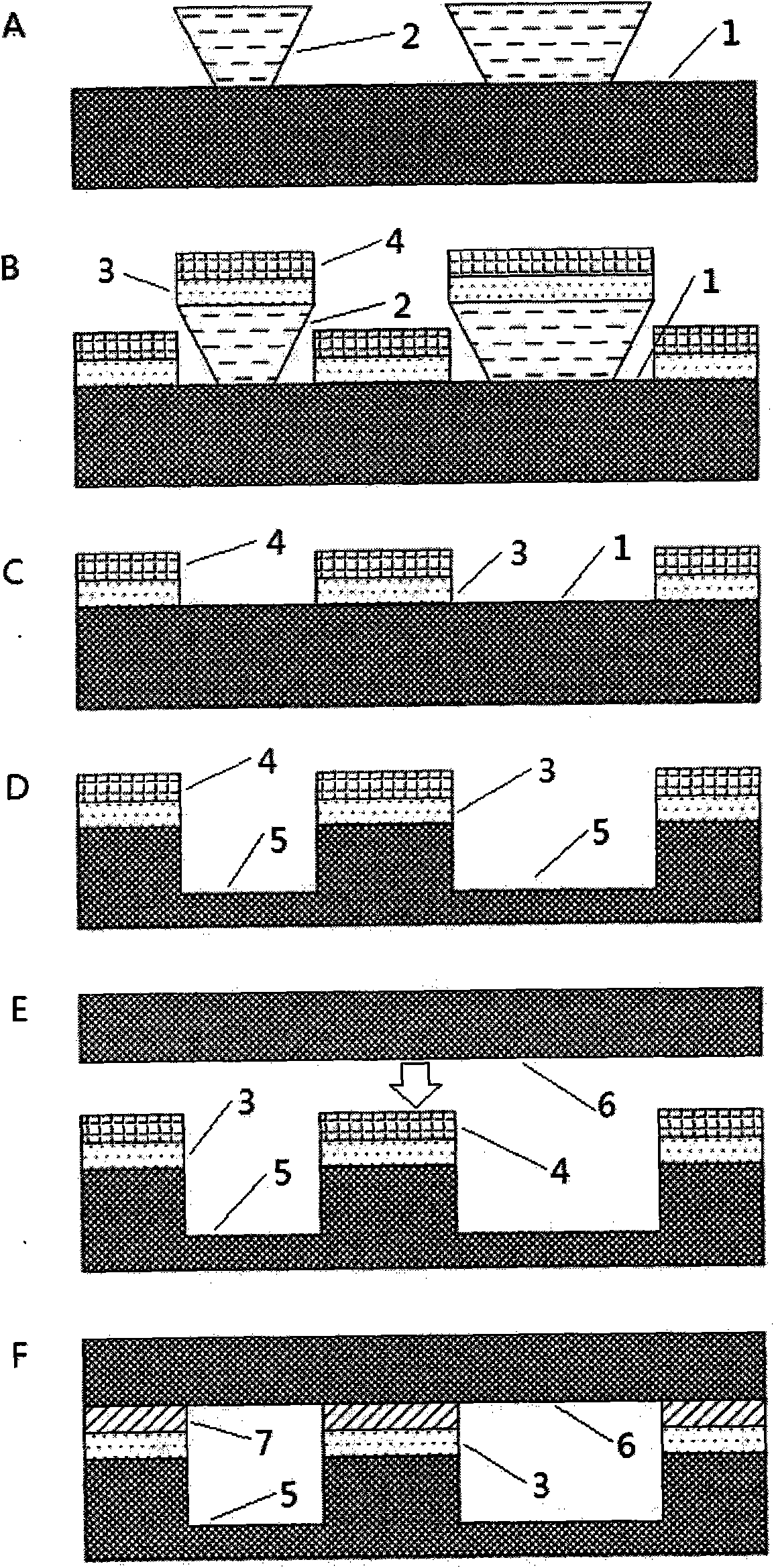
[0019] Embodiment 1 - micro gas enrichment device

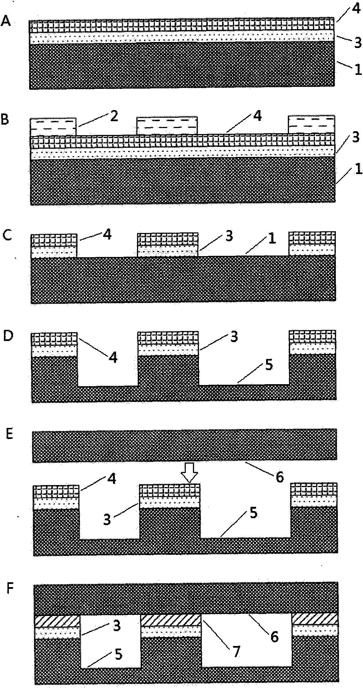
[0020] The micro gas concentrator etches several parallel deep grooves with vertical side walls on the silicon wafer, and then bonds a top cover on the front of the silicon wafer to complete the sealing of the grooves. In this embodiment, the Ti / Au film mask is prepared by the lift-off method, the silicon deep groove is etched by the wet etching method, and the gold-silicon bonding is used to complete the sealing. The specific steps are as follows: figure 2 Shown:

[0021] A) First, use a coating machine to evenly coat a layer of photoresist 2 (AZ6112) on (110) the first silicon wafer 1, and then align the window opening direction of the pattern on the photolithographic plate with the first silicon wafer 1. That is, the {111} crystal orientation group is precisely aligned and then exposed and developed, and the pattern on the photoresist plate is transferred to the photoresist 2, and the cross-sectional morphology of the ph...

Embodiment 2

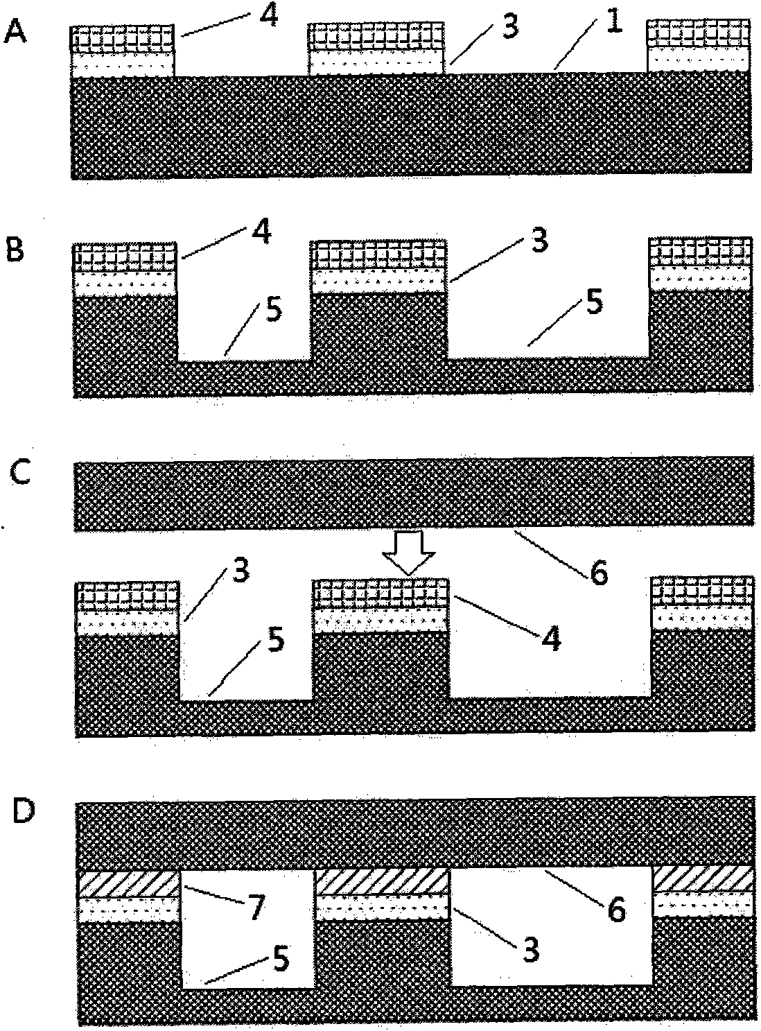
[0028] Embodiment 2-miniature gas chromatography column

[0029] The micro-gas chromatographic column is etched with a vertical deep groove on the silicon chip, and then a top cover is bonded on the front of the silicon chip to complete the sealing of the groove. The process flow of this embodiment is roughly as follows: first make a metal film layer, then perform photolithography and wet etching to form a metal mask, use dry etching to form a bulk silicon microstructure, and finally perform gold-silicon eutectic bonding. The specific steps Such as image 3 Shown:

[0030] A) On the cleaned first silicon wafer 1, a 50nm chromium film 3 and a 500nm gold film 4 are successively deposited by vacuum evaporation;

[0031] B) Exposure and development after spin-coating photoresist 2 to form a pattern;

[0032] C) using the photoresist 2 as an etching mask layer, corroding the gold film 4 and the chromium film 3 with a mixed solution of iodine+potassium iodide and tetraammonium ni...


PUM


Abstract

The invention discloses a bulk silicon etching and gold silicon bonding combined process method, which comprises the following steps of: firstly, forming a gold mask pattern on a first silicon wafer; secondly, dryly etching or wetly corroding the first silicon wafer by using a gold mask to form a bulk silicon microstructure; and finally, positioning a second silicon wafer on the first silicon wafer with a pattern structure to perform the gold silicon bonding. In the process method, a gold film layer is ingenuously used as a masking layer for forming the silicon microstructure in the etching process and also used as a bonding layer in a subsequent eutectic bonding process. In the traditional process, the etching of silicon and the bonding of the silicon wafer are two independent steps; while in the process method of the invention, the etching and the bonding are organically combined together, so that a process flow is simplified and production efficiency is improved.

Description

technical field [0001] The invention relates to a micro-electromechanical system (MEMS) manufacturing technology, in particular to a composite process method of bulk silicon etching and gold-silicon bonding. Background technique [0002] Bonding is an important processing method in MEMS technology. The use of bonding technology can reduce the complexity of single silicon chip processing, and realize complex channels, cavities and SOI. It is also an important packaging method. Bonding mainly includes silicon-glass bonding, silicon-silicon bonding, alloy bonding, etc. The more mature one is silicon-glass anode bonding. But to achieve a good anodic bonding, a large area of ​​silicon is required. For example, for a sealed structure, at least a "collar" of about 200um should be left around the cavity and recess. Alloy bonding only needs 1-3um to achieve a closed structure, so alloy bonding has attracted extensive attention in the industry in recent years. Alloy bonding is also...

Claims


Application Information

Patent Timeline
Patent Type & Authority Applications(China)
IPC IPC(8): B81C1/00
Inventor 杜晓松廖明杰王力蒋亚东严炎郝敏
Owner UNIV OF ELECTRONICS SCI & TECH OF CHINA
Why Eureka
Try Eureka