
Phthalocyanine rare earth organic infrared semiconductor light guide detector

A detector and semiconductor technology, applied in the field of optoelectronics, can solve the problems of few types of organic infrared semiconductors, low carrier mobility, high resistivity of photosensitive materials, etc., achieving considerable market prospects, controllable electrical parameters, and outstanding novelty Effect

Active Publication Date: 2012-07-25
KUNMING INST OF PHYSICS
View PDF0 Cites 0 Cited by
  • Summary
  • Abstract
  • Description
  • Claims
  • Application Information

AI Technical Summary

Problems solved by technology

At present, the practical quantum infrared detectors are mainly inorganic materials based on mercury cadmium telluride. The problems of these materials are: high preparation cost, complicated process, and cannot be prepared on cheap substrates, especially silicon substrates and metal electrodes. , thus limiting the application of infrared detectors with important military applications
[0005] So far, the basic and applied research on organic semiconductor materials and devices has mainly focused on organic light-emitting displays and organic photovoltaic solar cells. There are few research reports on organic infrared semiconductor materials and devices. At present, there are few types of organic infrared semiconductors that can be applied to detection less on the
Moreover, due to the van der Waals force between organic semiconductor molecules, the carrier mobility is low, the resistivity of photosensitive materials is large, and the properties are close to insulators, these factors limit the application of organic infrared semiconductors in the field of infrared detection.

Method used


Image

  • Phthalocyanine rare earth organic infrared semiconductor light guide detector
  • Phthalocyanine rare earth organic infrared semiconductor light guide detector
  • Phthalocyanine rare earth organic infrared semiconductor light guide detector

Examples


Embodiment 1

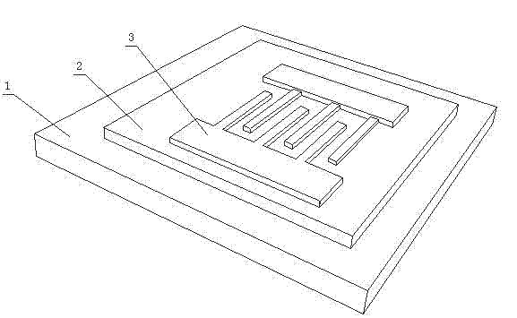
[0025] like image 3 As shown, the phthalocyanine rare earth organic infrared semiconductor detector with electrical controllability of the present invention includes: a substrate 1, and a metal or transparent conductive electrode 3 is prepared on the substrate by magnetron sputtering or electron beam evaporation method, Through the implementation of photolithography process, the electrode structure is made into interdigitated, serpentine, ring, strip, and spiral electrodes 2, and then the rare earth phthalocyanine is deposited on the electrode structure by solution casting, spin coating, printing or thermal evaporation Photosensitive layer 2; or on the substrate 1, deposit a rare earth phthalocyanine thin film by solution or thermal evaporation, then use a mask to cover the rare earth phthalocyanine thin film, and use thermal evaporation, electron beam evaporation or magnetron sputtering on the phthalocyanine Electrodes are deposited on rare earth films.

[0026] The materia...

Embodiment

[0037] A 30 nm Cr film and a 5 μm thick Au film were deposited on a quartz substrate by magnetron sputtering; a 2–3 μm thick photoresist was spin-coated on the Au film, and baked at 80°C for 5 minutes before drying under ultraviolet light. Exposure; form a certain strip pattern of the photoresist in the developer; bake the film at 80°C for 5 minutes to harden the film; use plasma etching or stripping technology to form the metal electrode into a strip pattern with a spacing of 3 μm; remove the photoresist , to obtain a metal electrode with a strip pattern on a quartz substrate; dissolve gadolinium phthalocyanine and iodine (mass ratio 95:5) in chloroform; drop the iodine-doped gadolinium phthalocyanine solution onto the metal strip electrode with a dropper, and wait until After the chloroform evaporates, the iodine-doped gadolinium phthalocyanine forms a film between the metal strip electrodes to form a device.

[0038] Example: 3

[0039] A 1 μm erbium phthalocyanine thin fi...


PUM


Abstract

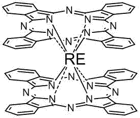
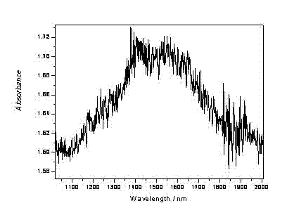
The invention relates to the technical field of photoelectron, in particular to a phthalocyanine rare earth organic infrared semiconductor light guide organic semi-conductor detector. The detector of the invention comprises a substrate, a metal or transparent conductive electrode, an organic infrared photosensitive material layer and the like. The detector is characterized in that the photosensitive material is phthalocyanine rare earth with a sandwich structure; the electrical parameters of the photosensitive material of the organic infrared semiconductor light guide detector are controllable, so that electric resistance of a device can be adjusted within a scope of three orders of magnitude by acceptor doping, the performance regulation of the device and the compatibility with the infrared system are enhanced; the photosensitive material is an organic infrared semiconductor material which can be used to fabricate a large-area and low-cost infrared photoconductive detector responsiveto infrared light with the wavelength of 1.3-1.8 micron on a silicon substrate integrated circuit, a cheap substrate glass, a quartz plate and a flexible plastic substrate and has the advantages of simple technology, low cost, controllable performances and the like.

Description

technical field [0001] The invention relates to the technical field of optoelectronics, in particular to a photoconductive organic semiconductor detector. Background technique [0002] Infrared detectors are one of the most important applications in infrared technology, and infrared detector materials are the direct factors that affect the performance of infrared detectors. The development of infrared materials can directly affect the performance and application of infrared detectors. At present, the practical quantum infrared detectors are mainly inorganic materials based on mercury cadmium telluride. The problems of these materials are: high preparation cost, complicated process, and cannot be prepared on cheap substrates, especially silicon substrates and metal electrodes. , thus limiting the application of infrared detectors with important military applications. [0003] Compared with inorganic semiconductor materials, organic semiconductor materials have the advantages...

Claims


Application Information

Patent Timeline
Patent Type & Authority Patents(China)
IPC IPC(8): H01L51/46H01L51/48
CPCY02E10/50Y02E10/549Y02P70/50
Inventor 唐利斌姬荣斌张筱丹段瑜宋立媛陈雪梅马钰
Owner KUNMING INST OF PHYSICS
Learn More