Organic ultraviolet light detection device based on Cu (I) coordination compound triplet-state material
An organic ultraviolet light and triplet technology, which is applied in the fields of semiconductor/solid-state device manufacturing, organic chemistry, electric solid-state devices, etc. The problem of single selection of bulk materials, etc., achieves the effect of low price, simple preparation method and simple synthesis method.
- Summary
- Abstract
- Description
- Claims
- Application Information
AI Technical Summary
Problems solved by technology
Method used
Image
Examples
preparation example Construction
[0033] Preparation of Cu(I) complex triplet material: 446.5mg (1.0mmol) 1,2-bis(diphenylphosphino)benzene, 314.0mg (1.0mmol)[Cu(CH 3 EN) 4 ] BF 4 Dissolve in 20ml of dichloromethane, stir at room temperature for about 30 minutes, then add 358.4mg (1.0mmol) of 2,9-dimethyl-4,-diphenyl-1,10-phenanthroline, and continue stirring for one hour; Filter, concentrate the filtrate to about 5ml, add 5ml CH 3 CN, Growth of single crystals by ether diffusion method.
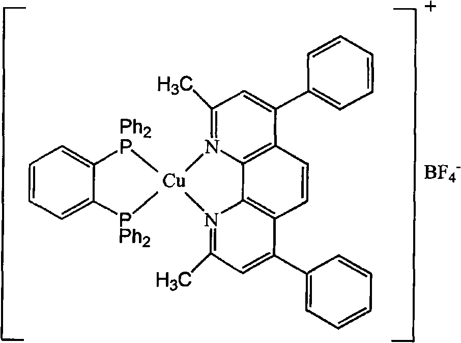
[0034] The structural formula of the described Cu(I) complex triplet material is:
[0035] [Cu(1,2-Bis(diphenylphosphino)benzene)(bathocuproine)]BF 4
[0036]
[0037] Among them: 1,2-Bis(diphenylphosphino)benzene is 1,2-bis(diphenylphosphino)benzene; bathocuproine is 2,9-dimethyl-4,7-diphenyl-1,10-phenanthrene Roline.
Embodiment 1
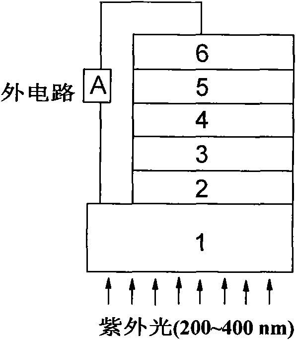
[0039] select figure 1 The device structure shown. In this embodiment, the electron donor layer m-MTDATA with a thickness of 30nm is firstly vacuum-deposited on the ITO conductive glass, and then the electron donor m-MTDATA and The mixed layer 3 of the electron acceptor Cu(I) complex has a thickness of 20nm, and the electron acceptor layer 4 is deposited on the mixed layer 3. The thickness of the Cu(I) complex triplet material is 40nm, and then the electron injection layer is deposited 5. The material is LiF with a thickness of 1nm; the last is the cathode, which is made of metal Al with a thickness of 120nm. All the above thin films are deposited by vacuum coating process. The thickness of the film is monitored by a film thickness monitoring instrument, and the external circuit is detected by KEITHLEY-2601.
[0040] Effect: with a light intensity of 0.691mW / cm 2 Irradiated by a UV lamp with a central wavelength of 365nm, the photocurrent response obtained at -10V is 248mA...
Embodiment 2
[0042] On the basis of Example 1, the electron donor layer TPD with a thickness of 20nm is vacuum deposited on the ITO conductive glass, and then on the electron donor layer 2, the electron donor TPD and electron acceptor Cu ( I) The mixed layer 3 of the complex has a thickness of 20nm, and other manufacturing conditions remain unchanged.
[0043] Effect: with a light intensity of 0.691mW / cm 2 Irradiated by a UV lamp with a central wavelength of 365nm, the photocurrent response obtained at -10V is 147mA / W, and the current density is 102μA / cm 2 .
PUM
| Property | Measurement | Unit |
|---|---|---|
| thickness | aaaaa | aaaaa |
| thickness | aaaaa | aaaaa |
| thickness | aaaaa | aaaaa |
Abstract
Description
Claims
Application Information


