Method and device for smelting and purifying polysilicon by using electron beams and adopting slag filtering

A technology of polysilicon and electron beams, applied in chemical instruments and methods, silicon compounds, inorganic chemistry, etc., can solve the problems of unfavorable popularization of solar cells, inability to effectively remove polysilicon at the same time, and inability to effectively remove polysilicon, etc., to increase the contact area Large size, high production efficiency, and the effect of increasing the reaction temperature

Inactive Publication Date: 2011-08-10
DALIAN LONGSHENG TECH CO LTD
View PDF7 Cites 17 Cited by
  • Summary
  • Abstract
  • Description
  • Claims
  • Application Information

AI Technical Summary

Problems solved by technology

However, the improved Siemens method and silane method require large equipment investment, high cost, serious pollution, and complicated processes, which are not conducive to the popular application of solar cells. In comparison, the metallurgical method has the characteristics of short production cycle, low pollution, and low cost. The focus of R&D in various countries
Electron beam smelting is one of the important methods for metallurgical purification of polysilicon. It can effectively reduce the impurity phosphorus in polysilicon, but most of the methods for purifying polysilicon by electron beam smelting cannot effecti

Method used


Image

  • Method and device for smelting and purifying polysilicon by using electron beams and adopting slag filtering
  • Method and device for smelting and purifying polysilicon by using electron beams and adopting slag filtering

Examples


Embodiment 1

[0025] A method for smelting and purifying polysilicon by electron beam and slag filtration. Firstly, a slag-forming agent is heated and melted by a graphite heating element in a smelting crucible to form a slag-forming agent melt, which is maintained in a liquid state. Slowly add high phosphorus, high boron and high metal polysilicon fragments, high phosphorus, high boron and high metal polysilicon fragments are melted into silicon melt under electron beam bombardment, and smelted to remove impurity phosphorus, after this low The phosphorus silicon melt enters the diversion device through the diversion port of the water-cooled copper crucible. The impurity boron in the silicon melt reacts with the slagging agent to remove the impurity boron. Finally, when the melt in the melting crucible is full, stop adding polysilicon material, and heat the melt in the melting crucible to keep it in a liquid state for 3 minutes, and finally pass The ingot pulling mechanism pulls the ingot d...

Embodiment 2

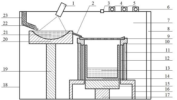
[0027] A kind of equipment for smelting and purifying polysilicon by electron beam and slag filtration. The equipment consists of a furnace door 8 and a vacuum furnace wall 2 to form a vacuum equipment. The inner cavity of the vacuum equipment is a vacuum chamber 7; A water-cooled ingot rod 17 is installed on the vacuum furnace wall 2 in the support base 16, the graphite block 15 is installed on the water-cooled ingot rod 17, the melting crucible 14 is placed on the graphite block 15, and the support base 16 is installed from the outside to the inside. The thermal insulation carbon felt 11 and the graphite heating element 12, the flow guide device is installed on the thermal insulation carbon felt 11 and the graphite heating element 12; the water-cooled support rod 19 is installed on the left side of the bottom of the vacuum chamber 7, and the water-cooled copper crucible 20 is installed on the water-cooled support rod 19 Above, the feeding device 23 is fixedly installed on the...

Embodiment 3

[0029] Adopt the equipment described in embodiment 2 to carry out the method for electron beam and slag filtration smelting purification polysilicon, its concrete steps are as follows:

[0030] The first step of material preparation: the mass percentage is SiO 2 70%, CaO20% and Na 2 CO 3 1200g of 10% slagging agent is spread on the bottom of the smelting crucible 14. At this time, the amount of slagging agent added is preferably 1 / 6 of the volume of the smelting crucible 14, and the furnace door 8 is closed;

[0031] The second step of pretreatment: use the mechanical pump 6 and the Roots pump 5 to pump the vacuum chamber 7 to a low vacuum of 7Pa, and then use the diffusion pump 4 to pump the vacuum chamber 7 to a high vacuum of 0.0015Pa; Put cooling water into the crucible 20 and the water-cooled ingot rod 17 to keep the temperature at 40°C; preheat the electron gun 1, set the high voltage to 30kV, and after the high voltage is stable for 5 minutes, turn off the high voltag...


PUM


Abstract

The invention belongs to the technical field of polysilicon purification adopting the physical metallurgy technology and provides a method for smelting and purifying polysilicon by using electron beams and adopting slag filtering. The method comprises the following steps: heating and melting a slag former in a melting crucible to form slag former melt, keeping the liquid state of the slag former melt while adding a high-phosphorus, high-boron and high-metal polysilicon material in a water cooled copper crucible by a charging device, melting the silicon material into silicon melt under the bombardment of the electron beams, removing impurity phosphorus through smelting; and leading the obtained low-phosphorus silicon melt to enter the slag former melt, removing the impurity boron by reacting the impurity boron of the silicon melt with the slag former in the fusing process, heating the melt in the melting crucible and keeping liquid smelting for 3-10 minutes after charging, performing directional solidification, and cutting the top waste residue of the silicon ingot and the high metal content silicon briquet to obtain the polysilicon product. The method comprehensively utilizes the technologies of electron beam smelting dephosphorization, slag filtering smelting boron removal and directional solidification metal removal to remove phosphorus, boron and metal impurities in polysilicon, thus the purification effect is good, the production efficiency is high and the method is suitable for mass production.

Description

technical field [0001] The invention belongs to the technical field of purifying polysilicon by physical metallurgy technology, and particularly relates to a method for removing impurity phosphorus, boron and metal in polysilicon; in addition, the invention also relates to the equipment thereof. Background technique [0002] Solar-grade polysilicon material is an important raw material for solar cells. Solar cells can convert solar energy into electrical energy. In today's shortage of conventional energy sources, solar energy has great application value. At present, the preparation of polysilicon materials for solar cells has formed a large-scale production worldwide, and the main technical routes are as follows: [0003] (1) Improved Siemens method: The Siemens method uses hydrochloric acid (or hydrogen, chlorine gas) and metallurgical grade industrial silicon as raw materials to perform hydrogen reduction from trichlorosilane. Now the relatively mature technology in forei...

Claims


Application Information

Patent Timeline
IPC IPC(8): C01B33/037
Inventor 谭毅战丽姝姜大川顾正邹瑞洵
Owner DALIAN LONGSHENG TECH CO LTD
Why Eureka
Try Eureka