Methods for manufacturing superjunction structure and superjunction semiconductor device

A technology of superjunction semiconductor and manufacturing method, which is applied in semiconductor/solid-state device manufacturing, electrical components, circuits, etc., can solve the problem of difficulty in accurately controlling the height of silicon dioxide in the expansion trench, increasing process complexity, and small process tolerance. problems, achieving superior performance, ease of filling and planarization, and increased process tolerances

Inactive Publication Date: 2011-08-10
UNIV OF ELECTRONICS SCI & TECH OF CHINA +1
View PDF5 Cites 16 Cited by
  • Summary
  • Abstract
  • Description
  • Claims
  • Application Information

AI Technical Summary

Problems solved by technology

However, after the active region (including body region, body contact region and source region) is formed, the process steps of small-tilt ion implantation, oxide filling and expanding trenches, and trench gate formation have the following main disadvantages: (1) process It is difficult to accurately control the height of silicon dioxide in the extended trench
On the one hand, the trench gate must span the body region in the vertical direction (that is, the upper surface of the oxide in the extended trench cannot be higher than the lower surface of the body region); on the other hand, the longer the trench gate overlaps with the drift region, the greater the gate-drain capacitance. The larger the is, and the withstand voltage of the device decreases with the decrease of the height of silicon dioxide in the extended trench, so it is necessary to accurately control the height of silicon dioxide in the extended trench to ensure the electrical performance of the device; (2) the higher the withstand voltage of the device, The deeper the extended trench, the more difficult the implantation, and the smaller the process tolerance; (3) In order to ensure that the ions implanted at a small inclination angle cover all areas below the active layer on both sides of the trench, and do not cover the active layer on both sides of the trench. layer, the mask for ion implantation is difficult to make, which increases the complexity of the process

Method used


Image

  • Methods for manufacturing superjunction structure and superjunction semiconductor device
  • Methods for manufacturing superjunction structure and superjunction semiconductor device
  • Methods for manufacturing superjunction structure and superjunction semiconductor device

Examples


Embodiment 1

[0063] As a preferred embodiment of the present invention, the present invention discloses a novel superjunction semiconductor device structure (such as Figure 4h Shown) the manufacturing method, it comprises the steps:

[0064] a. By epitaxial growth, a p-type semiconductor drift region 2 of the first conductivity type is formed on the semiconductor substrate 1, such as Figure 4a shown;

[0065] b. On the semiconductor drift region 2 of the first conductivity type, etch toward the semiconductor substrate along the top of the semiconductor drift region of the first conductivity type until the semiconductor substrate 1, forming a first trench ;Such as Figure 4b shown. Dry etching such as reactive ion etching may be used, or wet etching may be used. The aspect ratio of the trench can be accurately controlled by dry etching, and the formed trench is basically U-shaped; the trench formed by wet etching can be trapezoidal or V-shaped. Preferably, dry etching is selected to ...

Embodiment 2

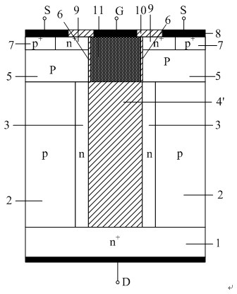
[0079] The manufacturing process of the semiconductor device of the present invention described in Embodiment 1 is preferably applied to a MOS control vertical device, so as to alleviate the contradictory relationship among withstand voltage, on-resistance and switching loss. Applied in such as Figure 5a when the IGBT device shown. The difference from Example 1 is that the initial semiconductor material substrate 1 is P + The semiconductor substrate 101 has the same conductivity type as the drift region of the first conductivity type. Its key steps are as Figure 5b shown. All the other steps are identical to Example 1.

Embodiment 3

[0081] The manufacturing process of the semiconductor device of the present invention described in Embodiment 1 can be applied to control vertical devices of N-channel MOS, and can also be applied to control vertical devices of P-channel MOS. P-channel VDMOS as Figure 6a shown. When used in the manufacture of P-channel MOS control vertical devices, the semiconductor substrate 1, the semiconductor layer 2 of the first conductivity type, the semiconductor drift region 3 of the second conductivity type formed by implantation at a small inclination angle, the active region 5, and the body contact region 7. The doping type of the source region 9 is opposite to that of the corresponding region of the N-channel MOS control vertical device. The key steps are as follows Figure 6b shown. In Embodiment 1, an N-channel VDMOS is manufactured, and N-type impurities are implanted at a small angle to form a semiconductor drift region 3 of the second conductivity type; A semiconductor dri...


PUM


Abstract

The invention discloses methods for manufacturing a superjunction structure and a superjunction semiconductor device. A novel semiconductor superjunction and a superjunction device are formed by the key process steps of etching a trench, performing ion implantation at a small inclination angle, filling an insulating dielectric and planarizing, forming an active layer and an electrode and the like. Compared with the prior art, the methods have the advantages that: firstly, a method of forming the superjunction by using a plurality of epitaxy processes and a plurality of implantation processes is prevented from being used; secondly, the bottom of a trench gate can be guaranteed to be flush with or slightly lower than the lower boundary of a body region, so that withstand voltage of the device is improved, and gate-source capacitance and gate-drain capacitance are reduced; thirdly, since the depth of the trench is reduced, the process difficulty of the small-angle implantation is reduced, the process tolerance is increased, and the dielectric in the extended trench is easier to fill and planarize; fourthly, a complex mask is not required, so that the influence of small-angle implantation on a trench region is avoided; and fifthly, the adverse effects of the filling and the planarizing of the extended trench and the manufacturing and the planarizing of the trench gate on the formed body region, body contact region and source region are avoided.

Description

[0001] technical field [0002] The invention relates to a manufacturing method of a super junction structure and a manufacturing method of a super junction semiconductor device. Background technique [0003] Power MOSFET is a multi-subconduction device, which has many advantages such as high input impedance, high frequency, and positive temperature coefficient of on-resistance. These advantages make it widely used in the field of power electronics, greatly improving the efficiency of electronic systems. [0004] The high voltage resistance of the device requires a long drift region and a low doping concentration in the drift region. However, as the length of the drift region increases and the doping concentration decreases, the on-resistance ( ) of the device increases, the on-state power consumption increases, and the on-resistance of the device R on There is the following relationship with the breakdown voltage BV: ie . [0005] With the advancement of the manufacturi...

Claims


Application Information

Patent Timeline
Patent Type & Authority Applications(China)
IPC IPC(8): H01L21/336H01L21/266H01L21/331
Inventor 罗小蓉姚国亮王元刚雷天飞葛瑞陈曦
Owner UNIV OF ELECTRONICS SCI & TECH OF CHINA
Why Eureka
Try Eureka