Nanoimprint based preparation method of LED with high light-emitting efficiency
A nano-imprinting and photoresist technology, which is applied in optical mechanical equipment, photo-engraving process of pattern surface, optics, etc., can solve the problems of inefficient cost, repeated use, and easy damage of the initial template, so as to improve the light output. Efficiency, low cost, cost reduction effect
- Summary
- Abstract
- Description
- Claims
- Application Information
AI Technical Summary
Problems solved by technology
Method used
Image

Examples
Embodiment 1
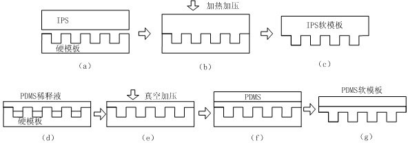
[0044] 1. Preparation of nano-imprint templates: Nano-imprint templates include hard templates and soft templates, which are described separately below.
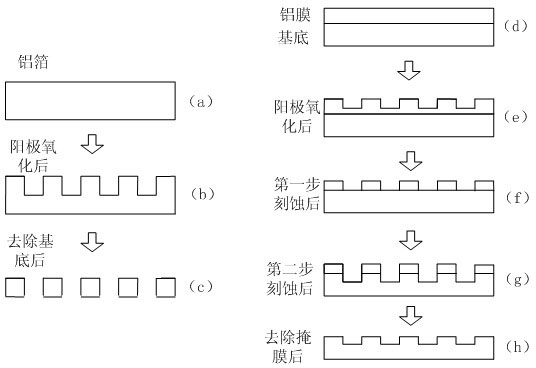
[0045] Preparation of hard template: (1) First, prepare the size, namely pore size, pore spacing, pore size, on pure aluminum (above 99.99%) by two-step electrochemical anodization in a 0.1-0.5mol / L oxalic acid, sulfuric acid or phosphoric acid solution. The depth-adjustable regular anodic aluminum oxide AAO template, the anode voltage is 20~200V, the temperature is 0~15℃, the first oxidation time is 2~5 hours, and the second oxidation time is 1~10 minutes. After step oxidation, the mass concentration of 5% H 3 PO 4 Perform hole expansion treatment in the process, and finally separate the aluminum substrate from the oxide layer to obtain the required through-hole alumina AAO hard template, such as figure 1 As shown in (c); (2) First, a layer of aluminum film is vapor-deposited on the surface of the flat substrate, the thickness ...
Embodiment 2
[0055] 1. Preparation of the nanoimprint template. The nanoimprint template includes a hard template and a soft template. The preparation process is the same as in Example 1.
[0056] 2. Preparation of the target piece:
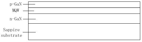
[0057] Clean the sapphire substrate first, and use metal organic chemical vapor deposition (MOVCD), molecular beam epitaxy (MBE) and other semiconductor epitaxial growth methods to sequentially grow different epitaxial layers on the sapphire substrate to obtain the epitaxial wafer. The target sheet, which includes at least a sapphire substrate, an N-type layer, an active layer and a P-type layer from bottom to top. Such as image 3 Shown
[0058] 3. Uniform glue: spin-coating a layer of UV curable photoresist STU2-120 on the surface of the target film, first rotate it at 500rpm for 10s, so that the hot press glue is evenly spread on the surface of the target film, and then at 3000~4500rpm Rotate for 30s at a speed of, to get rid of excess UV embossing glue, thinni...
Embodiment 3
[0064] 1. Preparation of the nanoimprint template. The nanoimprint template includes a hard template and a soft template. The preparation process is the same as in Example 1.
[0065] 2. Preparation of the target piece:
[0066] Clean the sapphire substrate first, use metal organic chemical vapor deposition (MOVCD), molecular beam epitaxy (MBE) and other semiconductor epitaxial growth methods to sequentially grow different epitaxial layers on the sapphire substrate to make an epitaxial wafer, and finally the epitaxial wafer A layer of SiO is deposited on the surface 2 Or Cr, SiO deposited 2 The thickness of the mask is 20~45nm, and the thickness of the Cr mask is about 10nm, so as to obtain the required target piece, which includes at least sapphire substrate, N-type layer, active layer, P-type layer and SiO from bottom to top. 2 Or Cr mask. Such as Figure 7 Shown
[0067] 3. Uniform glue: spin-coating a layer of mr-I7020E hot pressing glue on the surface of the target sheet, first...
PUM
| Property | Measurement | Unit |
|---|---|---|
| Thickness | aaaaa | aaaaa |
| Thickness | aaaaa | aaaaa |
| Thickness | aaaaa | aaaaa |
Abstract
Description
Claims
Application Information
 - R&D
- Intellectual Property
- Life Sciences
- Materials
- Tech Scout
- Unparalleled Data Quality
- Higher Quality Content
- 60% Fewer Hallucinations
Browse by: Latest US Patents, China's latest patents, Technical Efficacy Thesaurus, Application Domain, Technology Topic, Popular Technical Reports.
© 2025 PatSnap. All rights reserved.Legal|Privacy policy|Modern Slavery Act Transparency Statement|Sitemap|About US| Contact US: help@patsnap.com