
Cadmium sulfide thin film solar cell and preparation method thereof

A thin-film solar cell and cadmium sulfide technology, which is applied in circuits, photovoltaic power generation, electrical components, etc., can solve the problems of affecting the performance of the front electrode, incomplete copper diffusion, difficult control, etc., and achieve more stable photoelectric conversion efficiency and high photoelectric conversion Efficiency, the effect of eliminating lattice mismatch

Inactive Publication Date: 2011-09-14
SICHUAN UNIV
View PDF2 Cites 4 Cited by
  • Summary
  • Abstract
  • Description
  • Claims
  • Application Information

AI Technical Summary

Problems solved by technology

Formed by thermal diffusion p Type materials are difficult to determine the position of the barrier region, and CdS has a self-compensation effect, which is not easy to achieve p type doping, so that the prepared CdS is generally n type semiconductor
Therefore, by diffusion treatment to obtain p Type CdS is more difficult
In addition, at high temperature, copper will also diffuse to ITO, which will affect the performance of the front electrode. At the same time, the incomplete diffusion or residue of copper will also affect the transmission of sunlight.
[0004] In addition to the above-mentioned CdS-based solar cells, there is also a CdS-based solar cell made by the "Clevite process", that is, a CdS single crystal or thin film is used as a substrate, impregnated with hot Cu 2 Cl 2 solution, reaction p Type Cu 2 S, so as to obtain heterojunction CdS solar cells. Although the cost of this type of cell is relatively low, the efficiency of the cell is 5-8%, and large-scale production can be achieved, but this type of cell is difficult to control p type compound Cu x The phase of S is easy to produce a mixed phase, and at the same time, the battery is accompanied by a decay phenomenon
[0005] Therefore, the above two batteries have not achieved great development.

Method used


Image

  • Cadmium sulfide thin film solar cell and preparation method thereof
  • Cadmium sulfide thin film solar cell and preparation method thereof
  • Cadmium sulfide thin film solar cell and preparation method thereof

Examples


Embodiment 1

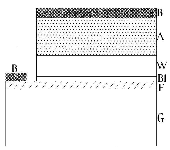
[0023] 1. On borosilicate glass (G), a commercial hot-pressed oxide target (SnO 2 : ~33 mol%, CdO: ~67%), the preparation of Cd 2 SnO 4 (F) Conductive layer. Sputtering conditions: background vacuum ~10 -5 Pa, the working atmosphere is 99.993% pure oxygen, the working pressure is 1-2 Pa, the distance between the target and the sample is 6-9 cm, the sputtering power is 100-600 W, and the sputtering thickness is 100-500 nm. After sputtering, the sample was taken out and placed in a CdS / Ar atmosphere at 580 0 C ~660 0 C heat treatment for 10~30 minutes.

[0024] 2. At room temperature, a commercial hot-pressed oxide target (SnO 2 : ~33 mol%, ZnO: ~67%), to prepare Zn 2 SnO 4 (B1). Sputtering conditions: background vacuum ~10 -5 Pa, the working atmosphere is 99.993% pure oxygen, the working pressure is 1~2 Pa, the distance between the target and the sample is 6~9 cm, the sputtering power is 100~600W, and the sputtering thickness is 70~300 nm.

[0025] 3. Take out str...

Embodiment 2

[0030] 1. On borosilicate glass (G), a commercial hot-pressed oxide target (SnO 2 : ~33 mol%, CdO: ~67%), the preparation of Cd 2 SnO 4 (F) Conductive layer. Sputtering conditions: background vacuum ~10 -5 Pa, the working atmosphere is 99.993% pure oxygen, the working pressure is 1-2 Pa, the distance between the target and the sample is 6-9 cm, the sputtering power is 100-600 W, and the sputtering thickness is 100-500 nm. After sputtering, the sample was taken out and placed in a CdS / Ar atmosphere at 580 0 C ~660 0 C heat treatment for 10~30 minutes.

[0031] 2. At room temperature, a commercial hot-pressed oxide target (SnO 2 : ~33 mol%, ZnO: ~67%), to prepare Zn 2 SnO 4 (B1). Sputtering conditions: background vacuum ~10 -5 Pa, the working atmosphere is 99.993% pure oxygen, the working pressure is 1-2 Pa, the distance between the target and the sample is 6-9 cm, the sputtering power is 100-600 W, and the sputtering thickness is 70-300 nm.

[0032] 3. Take out st...

Embodiment 3

[0037] Change the in-situ post-treatment in step 5 in embodiment one or embodiment two to non-in-situ post-treatment, that is, the sample is taken out, and under the protection of nitrogen or inert gas, heat treatment for 250 0 C ~400 0 C, the time is 10-30 minutes. The other steps are the same as in the first or second embodiment, and a cadmium sulfide homojunction solar cell can also be produced.


PUM

PropertyMeasurementUnit
Thicknessaaaaaaaaaa
Thicknessaaaaaaaaaa
Thicknessaaaaaaaaaa

Abstract

The invention belongs to the field of novel energy source materials and devices, in particular relates to a preparation method of a semiconductor film solar cell and provides a CdS homojunction solar cell structure, wherein Cd2SnO4 serves as a transparent conducting layer, n type CdS serves as a window layer, Zn2SnO4 serves as a buffering layer material between the transparent conducting layer and the window layer, and p type CdS serves as an absorbing layer. On the basis of the CdS homojunction solar cell structure, a CdS solar cell is prepared by a dry process. Namely, the preparation method comprises the following steps of: performing radio-frequency sputtering on the borosilicate or aluminosilicate glass to form the transparent conducting layer Cd2SnO4; performing radio-frequency sputtering to form the buffering layer Zn2SnO4; performing radio-frequency sputtering to form the n type CdS serving as the window layer; depositing copper-doped CdS at room temperature through physical gas phase method and performing post treatment to form the p type CdS serving as the absorbing layer; or directly growing the p type copper-doped CdS serving as the absorbing layer at a certain temperature through the physical gas phase method; and depositing a metal electrode and connecting a lead. Through the structure and the process, sun light can be better collected and used; p type doping treatment can be effectively performed on the CdS; influences caused by lattice mismatch and interface state are eliminated; and then higher photoelectric conversion efficiency is achieved.

Description

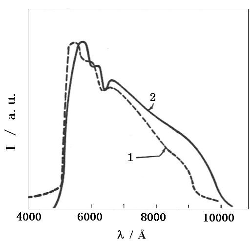
technical field [0001] The invention belongs to the field of new energy materials and devices, and in particular relates to a method for preparing a semiconductor thin film solar cell. Background technique [0002] Cadmium sulfide (CdS) is an important photosensitive semiconductor widely used in the field of optoelectronics, such as photoconductive gas sensors, photocells, semiconductor lasers, infrared detectors, solar cells, etc. [0003] An important application of CdS in the photovoltaic field is to make CdS solar cells. This type of solar cell is prepared with CdS as the base material. Because of its spectral response and solar spectrum match very well, it is suitable for solar cells and can obtain relatively high theoretical conversion. efficiency (see figure 1 ). In the 1950s, the structure of CdS solar cells that received great attention in the field of photovoltaics was: CdS / Cu / electrode, and its preparation method usually uses properly doped n Type CdS single cr...

Claims


Application Information

Patent Timeline
IPC IPC(8): H01L31/068H01L31/18
CPCY02E10/50Y02E10/547Y02P70/50
Inventor 李卫冯良桓张静全武莉莉蔡亚平谢晗科朱喆高静静
Owner SICHUAN UNIV
Learn More