AlGaN base deep ultraviolet light-emitting diode (LED) device using multiple quantum well electronic barrier layer to improve luminescent efficiency and manufacturing method of AlGaN base deep ultraviolet LED device

A technology of electron blocking layer and LED devices, which is applied in the direction of electrical components, semiconductor devices, circuits, etc., can solve the problems affecting the quantum efficiency of devices, low conductivity, and limited blocking ability, so as to improve the external quantum efficiency and increase the hole concentration Effect

Inactive Publication Date: 2011-09-14
武汉华炬光电有限公司
View PDF4 Cites 27 Cited by
  • Summary
  • Abstract
  • Description
  • Claims
  • Application Information

AI Technical Summary

Problems solved by technology

Because the blocking ability of the single-layer barrier is limited, although it can also have a good electron blocking effect in the visible light and UVA bands, for the UVB\UVC bands, due to the low conductivity of the p-type AlGaN material with high Al composition, As a result, the electron blocking layer of a single layer of high Al composition AlGaN ma

Method used


Image

  • AlGaN base deep ultraviolet light-emitting diode (LED) device using multiple quantum well electronic barrier layer to improve luminescent efficiency and manufacturing method of AlGaN base deep ultraviolet LED device
  • AlGaN base deep ultraviolet light-emitting diode (LED) device using multiple quantum well electronic barrier layer to improve luminescent efficiency and manufacturing method of AlGaN base deep ultraviolet LED device
  • AlGaN base deep ultraviolet light-emitting diode (LED) device using multiple quantum well electronic barrier layer to improve luminescent efficiency and manufacturing method of AlGaN base deep ultraviolet LED device

Examples


Embodiment Construction

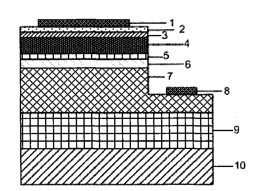
[0013] The fabrication of the device of the present invention includes two steps of material growth and device fabrication.

[0014] refer to figure 2 , the material growth steps of the present invention are as follows:

[0015] In step 1, a low-temperature AlN nucleation layer is grown on a sapphire substrate by MOCVD process.

[0016] The substrate temperature was lowered to 600°C, the growth pressure was maintained at 40Torr, the flow rate of hydrogen gas was 1500 sccm, the flow rate of ammonia gas was 1500 sccm, and the aluminum source with a flow rate of 28 μmol / min was introduced into the reaction chamber to grow a low-temperature AlN nucleation layer with a thickness of 20 nm.

[0017] Step 2, growing a high-temperature AlN intrinsic layer on the low-temperature AlN nucleation layer.

[0018]Raise the growth temperature to 1100°C, keep the growth pressure at 40Torr, the flow rate of hydrogen gas at 1500sccm, the flow rate of ammonia gas at 1500sccm, enter the aluminu...


PUM

PropertyMeasurementUnit
Thicknessaaaaaaaaaa
Thicknessaaaaaaaaaa
Thicknessaaaaaaaaaa

Abstract

The invention discloses a method for improving the luminescent efficiency of an AlGaN base deep ultraviolet light-emitting diode (LED) device. According to the method, a multi-cycle AlGaN quantum well structure is used as an electronic barrier layer to prevent electrons from escaping from an active region to a p-AlGaN potential barrier house. Compared with an ordinary single-layer AlGaN electronic barrier layer, the electronic barrier layer of the multiple AlGaN quantum well structure can more effectively reduce the electrons transmitted to a p type layer through a quantum interference effect so as to improve the injection efficiency of the electrons, and improve the luminescent efficiency of the LED device.

Description

technical field [0001] The invention belongs to the field of optoelectronic technology, and relates to a semiconductor device, in particular to a method for realizing a novel AlGaN-based multi-quantum well deep ultraviolet LED device, which can be used in the fields of water treatment, medical treatment, biomedicine and white light illumination. Background technique [0002] The research and development of semiconductor deep ultraviolet light-emitting diode (LED) is a research hotspot of wide bandgap semiconductor optoelectronic devices. The traditional ultraviolet light sources currently used are gas lasers and mercury lamps, which have disadvantages such as low efficiency, large volume, environmental protection and high voltage. On the contrary, the semiconductor ultraviolet light source is a solid-state ultraviolet light source, which has the advantages of high efficiency, long life, small size, light weight, environmental friendliness, low voltage, etc. Health and other...

Claims


Application Information

Patent Timeline
IPC IPC(8): H01L33/14H01L33/04H01L33/06H01L33/00
Inventor 陈莉蔡茜熊辉
Owner 武汉华炬光电有限公司
Why Eureka
Try Eureka