SiC IEMOSFET (Implantation and Epitaxial Metal-Oxide -Semiconductor Field Effect Transistor) device with epitaxy channel and manufacturing method of SiC IEMOSFET device

An epitaxy and channel technology, applied in the field of microelectronics, can solve the problems of rough contact interface, high interface state density, reduced electron mobility of the inversion layer, and increased device on-resistance, so as to reduce the roughness and suppress the contact interface Roughness, the effect of reducing the on-resistance

Active Publication Date: 2011-11-16
陕西半导体先导技术中心有限公司
View PDF3 Cites 28 Cited by
  • Summary
  • Abstract
  • Description
  • Claims
  • Application Information

AI Technical Summary

Problems solved by technology

[0005] Although the use of this structure and process improves the interface characteristics of the device to a certain extent, because the buried channel 6 of the device is still formed by ion implantation, the resulting SiC and SiO 2 A ser...

Method used


Image

  • SiC IEMOSFET (Implantation and Epitaxial Metal-Oxide -Semiconductor Field Effect Transistor) device with epitaxy channel and manufacturing method of SiC IEMOSFET device
  • SiC IEMOSFET (Implantation and Epitaxial Metal-Oxide -Semiconductor Field Effect Transistor) device with epitaxy channel and manufacturing method of SiC IEMOSFET device
  • SiC IEMOSFET (Implantation and Epitaxial Metal-Oxide -Semiconductor Field Effect Transistor) device with epitaxy channel and manufacturing method of SiC IEMOSFET device

Examples


Embodiment 1

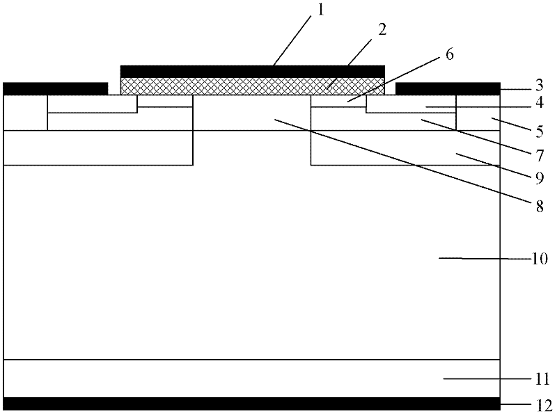
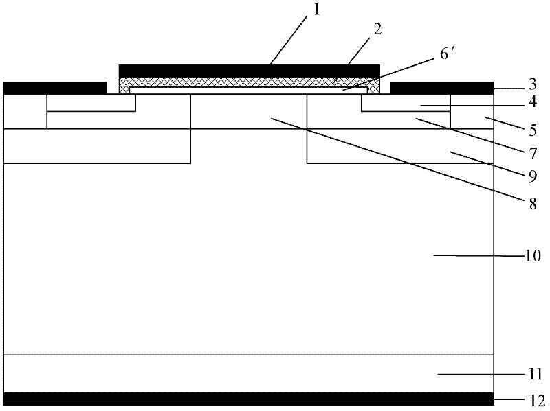
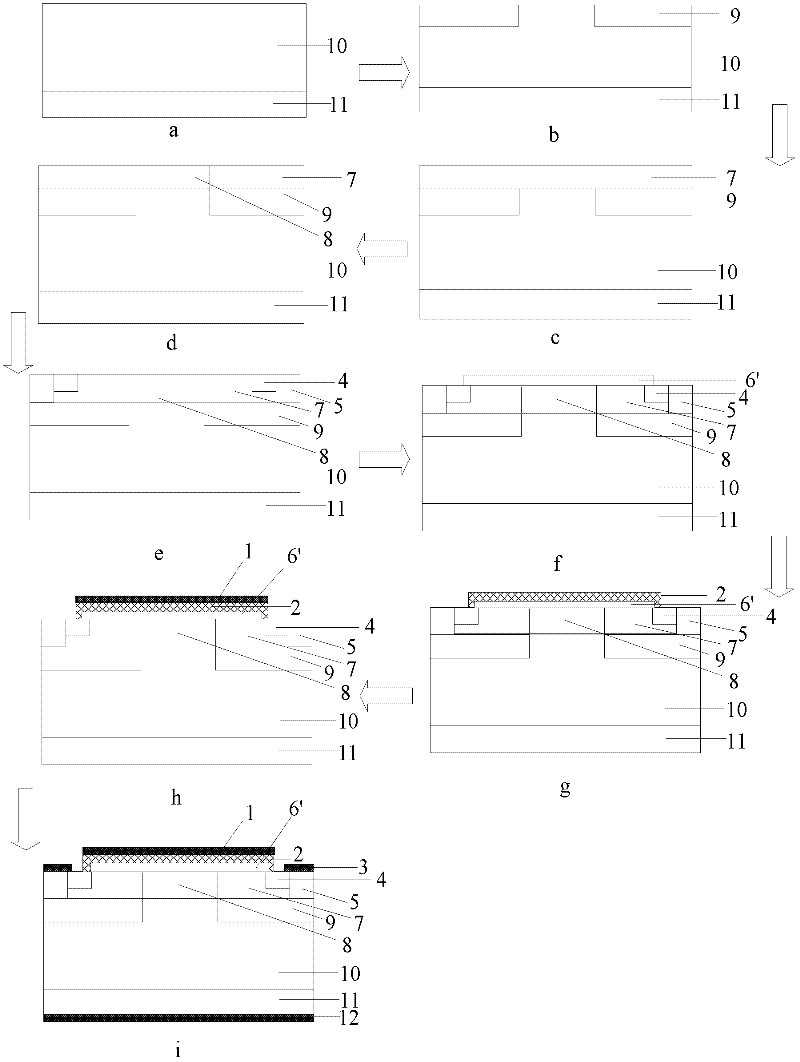
[0033] Step 1. In N + Epitaxial growth of N on SiC substrate samples - Drift layer.

[0034] to N + The silicon carbide substrate sample 11 was cleaned by RCA cleaning standard, and then epitaxially grown on the entire substrate surface with a thickness of 8 μm and a nitrogen ion doping concentration of 1×10 15 cm -3 N - Drift layer 10, such as image 3 a. The process conditions are as follows: the epitaxy temperature is 1570°C, the pressure is 100mbar, the reaction gas is silane and propane, the carrier gas is pure hydrogen, and the impurity source is liquid nitrogen.

[0035] Step 2. Selective implantation of aluminum ions four times to form a P well.

[0036] (2.1) Deposit a layer of Al with a thickness of 1.5 μm on the front side of the silicon carbide sample by low-pressure hot-wall chemical vapor deposition as a barrier layer for the ion implantation of the P well 9, and form the P well implantation region by photolithography and etching;

[0037] (2.2) Four times...

Embodiment 2

[0069] Step 1. In N + Epitaxial growth of N on SiC substrate samples - Drift layer.

[0070] to N + The silicon carbide substrate 11 is cleaned by RCA cleaning standard, and then the epitaxial growth thickness is 8.5 μm on the entire substrate surface, and the nitrogen ion doping concentration is 1.5×10 15 cm -3 N - Drift layer 10, such as image 3 a. The process conditions are as follows: the epitaxy temperature is 1570°C, the pressure is 100mbar, the reaction gas is silane and propane, the carrier gas is pure hydrogen, and the impurity source is liquid nitrogen.

[0071] The second step. Three times of selective implantation of aluminum ions to form a P well.

[0072] (2.1) Deposit a layer of Al with a thickness of 1.5 μm on the front side of the silicon carbide sample by low-pressure hot-wall chemical vapor deposition as a barrier layer for the ion implantation of the P well 9, and form the P well implantation region by photolithography and etching;

[0073] (2.2) Pe...

Embodiment 3

[0105] Step A. For N + The silicon carbide substrate 11 is cleaned by RCA cleaning standard, and then the epitaxial growth thickness is 9 μm on the entire substrate surface, and the nitrogen ion doping concentration is 2×10 15 cm -3 N - Drift layer 10, such as image 3 a, The epitaxial growth conditions are: the epitaxial temperature is 1570°C, the pressure is 100mbar, the reaction gas is silane and propane, the carrier gas is pure hydrogen, and the impurity source is liquid nitrogen.

[0106] Step B. Selective implantation of aluminum ions four times to form a P well.

[0107] (B1) Deposit a layer of Al with a thickness of 1.5 μm on the front side of the silicon carbide sample by low-pressure hot-wall chemical vapor deposition as a barrier layer for the ion implantation of the P well 9, and form the P well implantation region by photolithography and etching;

[0108] (B2) Perform Al ion implantation on the front side of the silicon carbide sample four times at an ambient ...


PUM

PropertyMeasurementUnit
Thicknessaaaaaaaaaa
Thicknessaaaaaaaaaa

Abstract

The invention discloses a SiC IEMOSFET (Implantation and Epitaxial Metal-Oxide -Semiconductor Field Effect Transistor) device with an epitaxy channel and a manufacturing method of the SiC IEMOSFET device, which mainly solve the problems of low channel electron mobility and high conductor resistance of the traditional SiC IEMOSFET device. The device disclosed by the invention comprises a grid electrode (1), a SiO2 insulating medium (2), a source electrode (3), a source region N<+> contact (4), a P<+> contact (5), a P<-> epitaxy layer (7), a JFET (Junction Field-effect Transistor) region (8), aP well (9), an N<-> drifting layer (10), an N<+> substrate (11) and a drain electrode (12), wherein an upper epitaxy channel layer (6') with the thickness of 0.1mum-0.2mum and the nitrogen ion dopingconcentration of 3*10<16>cm<-3> is arranged between the SiO2 insulating medium (2) and the JFET region (8) so that a conductive channel of the device in a working state is far away from SiO2 and SiCinterfaces and the impact of the surface scattering on the electron mobility is reduced. The SiC IEMOSFET device has the advantages of high channel electron mobility, low on-state resistance and low power dissipation and can be applied to fields such as switching mode voltage stabilizers, automotive electronics and power amplifiers.

Description

technical field [0001] The invention belongs to the technical field of microelectronics, and relates to a semiconductor device, in particular to a SiC IEMOSFET device with an epitaxial channel and a preparation method. Background technique [0002] SiC has become one of the most advantageous semiconductor materials for manufacturing high-temperature, high-power electronic devices due to its excellent physical, chemical and electrical properties, and has a power device quality factor much greater than that of Si materials. The research and development of SiC power device MOSFET began in the 1990s. It has a series of advantages such as high input impedance, fast switching speed, high operating frequency, and high temperature and high pressure resistance. It has been used in switching regulated power supplies, high-frequency heating, automotive electronics, and power amplifiers. and so on have been widely used. [0003] However, SiC and SiO in current SiC power MOSFET devices ...

Claims


Application Information

Patent Timeline
IPC IPC(8): H01L29/78H01L29/06H01L21/336H01L21/265
CPCH01L29/66068H01L29/7828
Inventor 汤晓燕张超张玉明张义门杨飞王文
Owner 陕西半导体先导技术中心有限公司
Why Eureka
Try Eureka