a solar cell
A technology for solar cells and electrodes, applied in the field of solar cells, can solve the problems of high reflectivity, expensive equipment, and no quantum size effect of nanomaterials.
- Summary
- Abstract
- Description
- Claims
- Application Information
AI Technical Summary
Problems solved by technology
Method used
Image
Examples
example 1
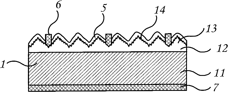
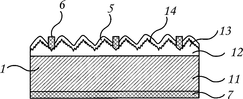
[0010] Example 1: Taking P-type single crystal silicon as an example: the silicon wafer after cutting will have a mechanical damage layer on the surface of the silicon wafer. Remove the damaged layer on the surface by high-concentration alkali washing, and then use a mixed solution of low-concentration alkali and alcohol to etch the surface of the silicon wafer to form a pyramid-structured suede on the surface of the silicon wafer, and then use phosphorus oxychloride at 860 ° C. Phosphorus is diffused to prepare PN junction, and then etching method is used to prepare silicon nano-layer, and then dry plasma is used to etch the edge of silicon wafer to prevent edge leakage, then hydrofluoric acid is used to remove phosphosilicate glass, and then enhanced plasma chemical vapor deposition The method deposits a silicon nitride film to form a passivation layer on the surface of the battery, or an anti-reflection layer, then screen-prints the back electrode to form a back electric fie...
PUM
| Property | Measurement | Unit |
|---|---|---|
| Size | aaaaa | aaaaa |
Abstract
Description
Claims
Application Information

