
A construction method of zno micro/nano material flexible strain sensor

A strain sensor and nanomaterial technology, applied in the construction of ZnO micro/nano material flexible strain sensors, can solve the problems of unsuitability for mass production and complicated operation, and achieve the effects of prolonging life, good crystallinity and overcoming brittleness

Inactive Publication Date: 2011-12-21
UNIV OF SCI & TECH BEIJING
View PDF5 Cites 16 Cited by
  • Summary
  • Abstract
  • Description
  • Claims
  • Application Information

AI Technical Summary

Problems solved by technology

However, such studies are usually carried out with the aid of atomic force microscopy (AFM) or nanomanipulation systems
These devices have relatively high requirements on the environment and materials, and the operation is complicated, so they are not suitable for mass production.

Method used

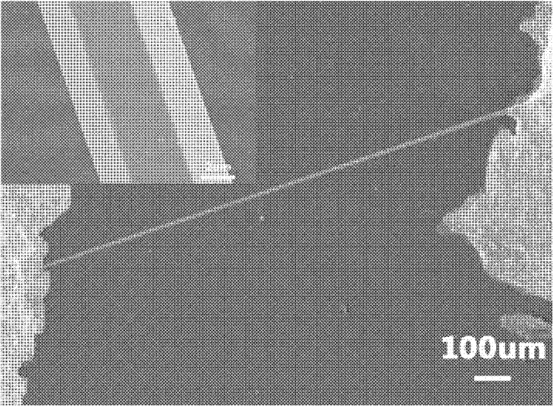
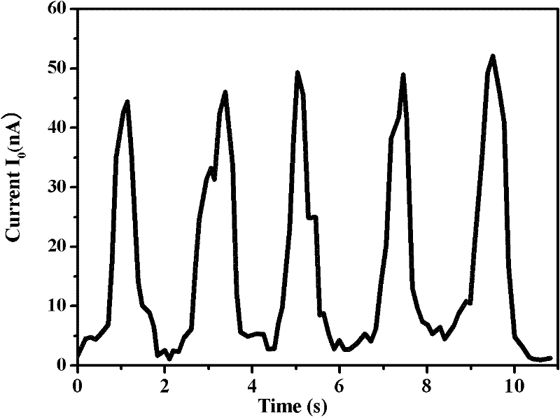

Image

  • A construction method of zno micro/nano material flexible strain sensor
  • A construction method of zno micro/nano material flexible strain sensor
  • A construction method of zno micro/nano material flexible strain sensor

Examples


Embodiment 1

[0026] First, the silicon substrate was rinsed with deionized water and alcohol, and dried at 40°C. An 8nm thick gold film was sprayed on the surface of the silicon wafer. Mix Zn powder (purity>99.9%) and C powder at an atomic ratio of 1:1, grind them thoroughly and place them in a porcelain boat, and put the silicon substrate upside down on the porcelain boat. Put the porcelain boat into the middle of the quartz tube in the tube furnace, adjust the flow meter to feed argon: oxygen = 50:1 into the tube. Under this atmosphere, the temperature of the tube furnace was raised to 970° C. and kept for 30 minutes to complete the preparation of the ZnO micro / nano material. Then, the ZnO micro / nano material was dispersed on the silicon wafer, the micro / nanowire ZnO was transferred onto the PDMS substrate by contact printing method, the two ends of the micro / nanowire ZnO were fixed with silver glue, and dried at 120 °C 30min. Finally, the PDMS was coated on the surface of the electro...

Embodiment 2

[0028] First, the silicon substrate was rinsed with deionized water and alcohol, and dried at 40°C. An 8nm thick gold film was sprayed on the surface of the silicon wafer. Mix Zn powder (purity >99.9%) and C powder according to the atomic ratio, grind them thoroughly and place them in a porcelain boat, and put the silicon substrate upside down on the porcelain boat. Put the porcelain boat into the middle of the quartz tube in the tube furnace, adjust the flow meter to feed argon: oxygen = 50:1 into the tube. Under this atmosphere, the temperature of the tube furnace was raised to 970° C. and kept for 30 minutes to complete the preparation of the micro / nano material ZnO. Then, the micro / nano material ZnO was dispersed on the silicon wafer, the micro / nano wire ZnO was transferred to the PI film substrate by contact printing method, the two ends of the micro / nano wire ZnO were fixed with silver glue, and heated at 120 °C. Dry for 30min. Finally, PDMS was coated on the surface ...


PUM

PropertyMeasurementUnit
lengthaaaaaaaaaa
diameteraaaaaaaaaa
lengthaaaaaaaaaa

Abstract

The invention discloses a construction method of a flexible strain sensor based on ZnO micro / nano material, and relates to the technical fields of nanotechnology and semiconductor device manufacturing. The strain sensor provided by the invention includes: ZnO single crystal micro / nano material, silver electrode, encapsulation layer polydimethylsiloxane (PDMS) and flexible substrate (PDMS, polyimide PI thin film). Among them, the ZnO single crystal micro / nano material with a length of 2-8 mm and a diameter of 0.5-5 μm is prepared by a vapor phase method and transferred to a flexible substrate by a contact printing method. The packaged device can be used in corrosive environments such as acid / alkali, and has a high degree of fit for working surfaces with different roughnesses, and has a high signal response to small strains. It can be used for bridge detection, automobile shock absorption detection and biomedical devices, etc.

Description

[0001] technical field [0002] The invention relates to the technical fields of nanotechnology and semiconductor device manufacturing, in particular to a construction method of a ZnO micro / nano material flexible strain sensor. Background technique [0003] With the continuous development of national defense, medical equipment, and electronics industries, research in the field of microcomputer / nanomachine systems (MEMS / NEMS) is showing rapid growth. One-dimensional nanomaterials, including nanowires / rods, nanoribbons, nanoneedles, nanocoaxial cables, and nanotubes, have unique electrical, mechanical, optical, and interactive coupling effects among them, and are considered to be the next-generation The foundation of a generation of electronic, optoelectronic, and nanoelectromechanical devices. Zinc oxide is a typical semiconductor material with direct bandgap and wide bandgap. It has special electrical and thermal conductivity, and its chemical properties are very stable. A...

Claims


Application Information

Patent Timeline
Patent Type & Authority Applications(China)
IPC IPC(8): B81C1/00
Inventor 张跃李萍廖庆亮张铮马斯威
Owner UNIV OF SCI & TECH BEIJING
Learn More