A method for encapsulating an optoelectronic device

A technology for optoelectronic devices and packaging methods, applied in the field of optoelectronics, can solve the problems of device performance degradation, stability degradation, and formation of black spots, and achieve the effects of extending device life, simplifying processes, and improving device stability.

Inactive Publication Date: 2011-12-28
UNIV OF ELECTRONIC SCI & TECH OF CHINA
View PDF6 Cites 3 Cited by
  • Summary
  • Abstract
  • Description
  • Claims
  • Application Information

AI Technical Summary

Problems solved by technology

Oxygen oxidizes organic materials to generate carbonyl compounds, which are serious quenchers. In addition, black spots will be formed when materials deteriorate, accompanied by device performance

Method used


Image

  • A method for encapsulating an optoelectronic device
  • A method for encapsulating an optoelectronic device
  • A method for encapsulating an optoelectronic device

Examples


Embodiment 1

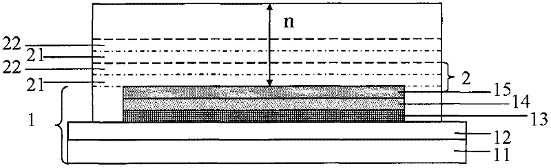
[0028] Such as figure 1 As shown, 1 is an organic electroluminescent device, the anode layer 12 is ITO, and the hole transport layer 13 is N, N'-bis(naphthylidene-1-yl)-N,N'-bis(phenyl) - benzidine (NPB), electron transport layer 14 is 1,3,5-(tri-N-phenyl-2-benzimidazole-2) benzene 41 (TPBi), cathode layer 15 is Mg:Ag alloy, inorganic thin film Packaging material layer 21 is Al 2 o 3 , UV-curable resin 22 includes 55% epoxidized octadecyl-conjugated triene-9,11,13-acid triglyceride, 4% glycerol, 0.98% lead oxide, 5% toluene di Isocyanate, 8% trimethylol propane, 0.01% hydroquinone, 12% tetrahydrofuran, 6% 2-hydroxyethyl methacrylate, 0.01% dibutyltin dilaurate, 1% 2, 2-dimethoxy-phenyl ketone and 8% methyl methacrylate, the number of cycles n is 20, the device structure is:

[0029] Glass substrate / ITO / NPB(50nm) / TPBi(30nm) / Mg:Ag(200nm) / [Al 2 o 3 (200nm) / UV curable resin (100nm)] 20

[0030] The preparation method is as follows:

[0031] ①Use detergent, acetone solutio...

Embodiment 2

[0039] Such as figure 1 As shown, 1 is an organic electroluminescent device, the anode layer 12 is ITO, and the hole transport layer 13 is N, N'-bis(naphthylidene-1-yl)-N,N'-bis(phenyl) - benzidine (NPB), electron transport layer 14 is 1,3,5-(tri-N-phenyl-2-benzimidazole-2) benzene 41 (TPBi), cathode layer 15 is Mg:Ag alloy, inorganic thin film Packaging material layer 21 is Al 2 o 3, UV-curable resin 22 includes 55% epoxidized octadecyl-conjugated triene-9,11,13-acid triglyceride, 4% glycerol, 0.01% lead oxide, 5% toluene di Isocyanate, 8% trimethylol propane, 0.989% hydroquinone, 12% tetrahydrofuran, 6% 2-hydroxyethyl methacrylate, 0.01% dibutyltin dilaurate, 1% 2, 2-dimethoxy-phenyl ketone and 8% methyl methacrylate, the number of cycles n is 16, the device structure is:

[0040] Glass substrate / ITO / NPB(50nm) / TPBi(30nm) / Mg:Ag(200nm) / [Al 2 o 3 (200nm) / UV curable resin (100nm)] 16

[0041] The preparation method is similar to Example 1.

Embodiment 3

[0043] Such as figure 1 As shown, 1 is an organic electroluminescent device, the anode layer 12 is ITO, and the hole transport layer 13 is N, N'-bis(naphthylidene-1-yl)-N,N'-bis(phenyl) - benzidine (NPB), electron transport layer 14 is 1,3,5-(tri-N-phenyl-2-benzimidazole-2) benzene 41 (TPBi), cathode layer 15 is Mg:Ag alloy, inorganic thin film Packaging material layer 21 is Al 2 o 3 , UV-curable resin 22 includes 30% epoxidized octadecaconjugated triene-9,11,13-acid triglyceride, 5% glycerol, 1% lead oxide, 7% toluene di Isocyanate, 10% trimethylol propane, 1% hydroquinone, 15% tetrahydrofuran, 10% 2-hydroxyethyl methacrylate, 1% dibutyltin dilaurate, 8% 2, 2-dimethoxy-phenyl ketone and 12% methyl methacrylate, the number of cycles n is 12, and the device structure is:

[0044] Glass substrate / ITO / NPB(50nm) / TPBi(30nm) / Mg:Ag(200nm) / [Al 2 o 3 (200nm) / UV curable resin (100nm)] 12

[0045] The preparation method is similar to Example 1.


PUM


Abstract

The invention discloses a method for encapsulating an optoelectronic device. The prepared device is encapsulated by a thin film encapsulation method. The thin film encapsulation layer covers the optoelectronic device. Overlapping composition, the UV-curable resin includes the following components: epoxidized octadecyl conjugated triene-9,11,13-acid triglyceride, glycerol, lead oxide, toluene diisocyanate, trimethyl alcohol Propane, hydroquinone, tetrahydrofuran, 2-hydroxyethyl methacrylate, dibutyltin dilaurate, 2,2-dimethoxy-phenyl ketone and methyl methacrylate. The packaging method can effectively block oxygen and water in the surrounding environment, which is beneficial to improve the stability of the device and prolong the life of the device; meanwhile, the packaging method has the characteristics of simple preparation process and low cost.

Description

technical field [0001] The invention relates to the field of optoelectronic technology, in particular to a packaging method for an optoelectronic device. Background technique [0002] Optoelectronics technology is a rapidly developing industry with high technological content after microelectronics technology. With the rapid development of optoelectronic technology, optoelectronic products such as light-emitting diodes, organic light-emitting diodes, solar cells, and thin-film transistors have gradually matured, and they have greatly improved people's lives. At the same time, the wide application of optoelectronic information technology in various fields of social life has also created a huge growing market, and the competition in the field of optoelectronic information is unfolding worldwide. [0003] Current optoelectronic devices, including organic electroluminescent devices, inorganic light emitting diodes, organic solar cells, inorganic solar cells, organic thin film tr...

Claims


Application Information

Patent Timeline
IPC IPC(8): H01L23/29H01L51/00C08G18/67C08F283/00
Inventor 于军胜陈珉张磊蒋亚东
Owner UNIV OF ELECTRONIC SCI & TECH OF CHINA
Why Eureka
Try Eureka