Method and device for preparing polycrystalline silicon solar cell texture

A solar cell and polysilicon technology, applied in circuits, electrical components, manufacturing tools, etc., can solve problems affecting processing quality and use effects, achieve high-quality and efficient suede processing, improve suede preparation efficiency, and high repeatability.

Inactive Publication Date: 2012-01-18
NANTONG UNIVERSITY
View PDF5 Cites 5 Cited by
  • Summary
  • Abstract
  • Description
  • Claims
  • Application Information

AI Technical Summary

Problems solved by technology

However, laser etching will cause thermal stress and mechanical damage to the substrate material of polycrystalline silicon solar cells, as well as a recast layer formed by redeposition of material spatter in the processing area, which affects the processing quality and use effect.

Method used


Image

  • Method and device for preparing polycrystalline silicon solar cell texture
  • Method and device for preparing polycrystalline silicon solar cell texture

Examples


Embodiment 1

[0031] The suede preparation of the polycrystalline silicon chip of the present embodiment carries out the preparatory work of following steps:

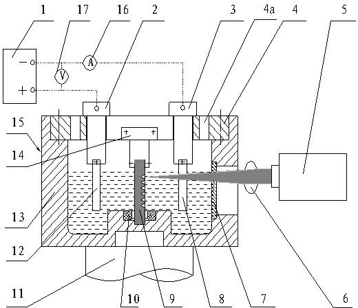
[0032] 1) Device assembly: an excimer laser with a wavelength of 193nm is used, the laser beam emitted is a pulsed laser, the beam transverse mode is a low-order mode, and the electrolysis voltage provided by the power supply is 5~8V; the polysilicon wafer with a thickness of 300 microns Connect and install to the corresponding part of the electrolyzer base 13.

[0033] 2) Inject electrolyte: slowly inject KOH electrolyte into the two chambers through the two liquid inlet vent holes on the cover plate 4 of the electrolytic cell. The pH value of the electrolyte is 9, the concentration is 20%, and the liquid level is slightly higher than The workpiece area to be processed is lower than the lower ends of the workpiece mounting fixture 14, the anode socket 2, and the cathode socket 3;

[0034] 3) Optical path detection: confirm that the...

Embodiment 2

[0041] The suede preparation of the polycrystalline silicon chip of the present embodiment carries out the preparatory work of following steps:

[0042] 1) Device assembly: a semiconductor laser with a wavelength of 532nm is used, the laser beam emitted is a continuous laser, the beam transverse mode is a low-order mode, and the electrolysis voltage provided by the power supply is 2~5V; the polysilicon wafer with a thickness of 250 microns is connected Install to the corresponding part of the electrolyzer base 13.

[0043] 2) Inject electrolyte: slowly inject KOH electrolyte into the two chambers respectively through the two liquid inlet vent holes of the electrolytic cell cover plate 4. The pH value of the electrolyte is 9.5, the concentration is 25%, and the liquid level is slightly higher than The workpiece area to be processed is lower than the lower ends of the workpiece mounting fixture 14, the anode socket 2, and the cathode socket 3;

[0044] 3) Optical path detection...

Embodiment 3

[0051] The suede preparation of the polycrystalline silicon chip of the present embodiment carries out the preparatory work of following steps:

[0052] 1) Device assembly: use a Nd:YAG laser with a wavelength of 1064nm, the transverse mode of the beam is a low-order mode, and the electrolysis voltage provided by the power supply is 5~8V; connect and install a polysilicon wafer with a thickness of 300 microns to the base of the electrolytic cell 13 corresponding parts.

[0053] 2) Inject electrolyte: slowly inject NaOH electrolyte into the two chambers through the two liquid inlet vent holes of the electrolytic cell cover plate 4. The pH value of the electrolyte is 10, the concentration is 30%, and the liquid level is slightly higher than The workpiece area to be processed is lower than the lower ends of the workpiece mounting fixture 14, the anode socket 2, and the cathode socket 3;

[0054] 3) Optical path detection: confirm that the optical path is smooth, the focusing len...


PUM

PropertyMeasurementUnit
Wavelengthaaaaaaaaaa
Thicknessaaaaaaaaaa
Wavelengthaaaaaaaaaa

Abstract

The invention relates to a method and device for preparing a polycrystalline silicon solar cell texture. The method comprises the following steps of: compositely machining a polycrystalline silicon wafer by using laser and electrochemistry; forming an array light trapping structure on the machined surface of the polycrystalline silicon wafer; meanwhile, generating electrochemical corrosion to thesurface of the polycrystalline silicon wafer by using electrolyte; and carrying out smooth finishing on the machined surface. The device for realizing the method comprises a laser 5 and an electrolysis mechanism 15 as well as a power supply 1 and a workbench 11, wherein the electrolysis mechanism 15 mainly comprises an electrolytic cell base 13, an electrolytic cell cover plate 4, a cathode 8, ananode 12, a workpiece mounting fixture 14, a sealing ring 10 and an optical protective mirror; the polycrystalline silicon wafer is placed in the electrolytic cell and the electrolytic cell is divided into two chambers so that the electrolytic cell is an unique current channel during electrolysis. The invention provides a novel highly efficient texture machining method of the polycrystalline silicon solar cell; and the product has the advantages of high repeatability, good height to width aspect ratio performance and important effect on increasing the photoelectric conversion efficiency; and the reflection reducing effect which is superior to the reflection reducing effect of the texture prepared through pure chemical corrosion can be obtained.

Description

technical field [0001] The invention relates to a method for fabricating the textured surface of polycrystalline silicon solar cells, in particular to a composite textured method using laser and electrochemical methods, and also relates to a special processing device for the method. Background technique [0002] Solar energy is the most important renewable energy source for human beings. A solar cell made of the Photovoltaic Effect is a device that can directly convert sunlight into electrical energy. Photovoltaic power generation has the advantages of safety and reliability, no noise, zero pollution emissions, less constraints, low failure rate, and easy maintenance. Silicon-based materials are the raw materials for making solar cells. According to the different materials used, solar cells can be divided into monocrystalline silicon solar cells, polycrystalline silicon solar cells, polycrystalline silicon thin-film solar cells, etc. Among them, the application proportion of...

Claims


Application Information

Patent Timeline
IPC IPC(8): H01L31/18B23K26/36C25F3/12
CPCY02P70/50
Inventor 张华花国然居志兰王强
Owner NANTONG UNIVERSITY
Why Eureka
Try Eureka