

Method for doping silicon wafer with colloidal silicon nano particles
A nanoparticle and colloidal silicon technology, applied in diffusion/doping, chemical instruments and methods, semiconductor/solid-state device manufacturing, etc., can solve the problems of complex equipment, high price, low production efficiency, etc., and achieve process simplification and simplicity The effect of selection doping
- Summary
- Abstract
- Description
- Claims
- Application Information
AI Technical Summary
Problems solved by technology
Method used
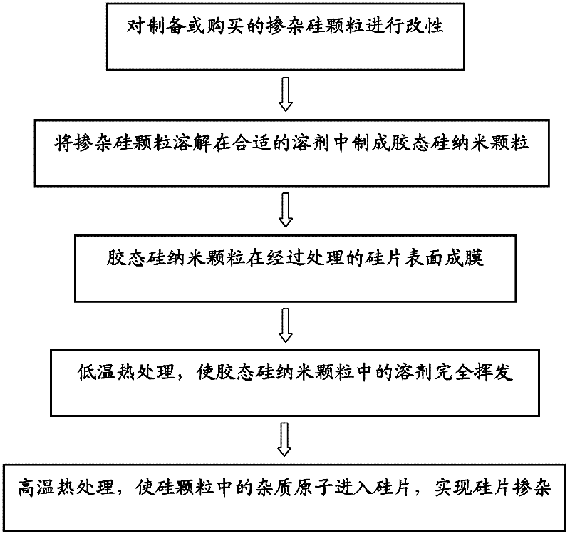
Image

Examples
Embodiment 1
[0030] Obtain phosphorus-doped silicon particles of 18 nanometers whose surface is passivated by hydrogen from the plasma preparation system of silicon particles. The standard deviation of the size distribution of silicon particles is 9% of the average size, and the atomic percentage of phosphorus doping in silicon particles is 5%. The phosphorus-doped silicon particles are placed in air, and they oxidize naturally at room temperature. After 60 days of natural oxidation, put the phosphorus-doped silicon particles with an oxide film on the surface into a mixed solution of ethanol and water (the volume ratio of ethanol and water is 5:2), and use a shear emulsifier to make the phosphorus-doped silicon particles as much as possible. dispersion. At a shear rate of 2000r / min and a reaction temperature of 70°C, 25% by mass of the silane coupling agent CH 2 =C(CH 3 )COO(CH 2 ) 3 Si(OCH 3 ) 3, adjust the pH value of the system to about 4 with oxalic acid solution, and obtain pho...
Embodiment 2
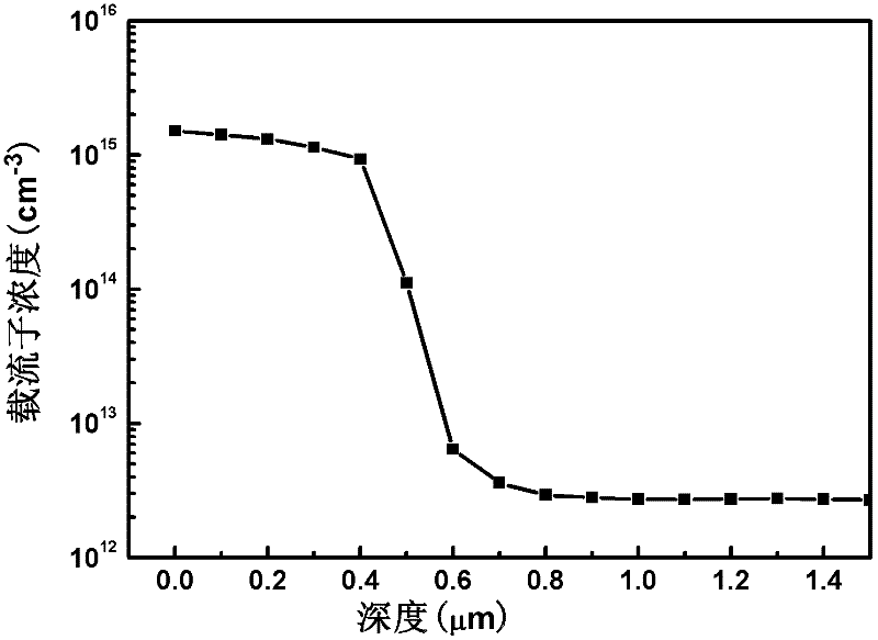
[0032] Obtain phosphorus-doped silicon particles of 44 nanometers surface passivated by hydrogen from the plasma preparation system of silicon particles. The standard deviation of the size distribution of silicon particles is 15% of the average size, and the atomic percentage of phosphorus doping in silicon particles is 8%. Put phosphorus-doped silicon particles in a mixed solution of ethanol and acrylic acid (the volume ratio of ethanol and acrylic acid is 3:1), and carry out hydrosilylation reaction under ultraviolet radiation until the mixed solution becomes clear, so as to obtain the surface through Modified silicon particles. The surface-modified phosphorus-doped silicon particles are separated from the mixed solution by centrifugal separation, and then dispersed in ethanol to obtain colloidal silicon nanoparticles. The concentration of silicon particles in the obtained colloidal silicon nanoparticles was 20% (wt). Soak a 1.5 cm x 1.5 cm N-type undoped silicon wafer in ...
Embodiment 3
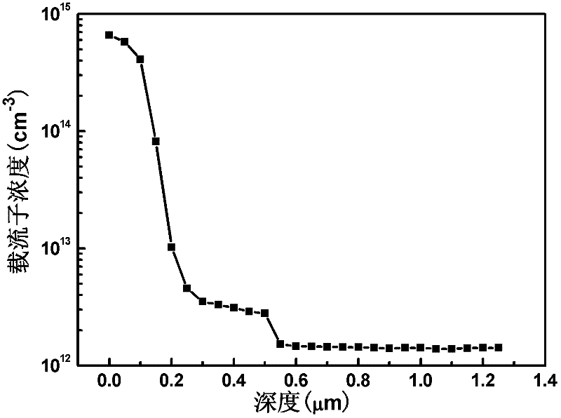
[0034] Obtain phosphorus-doped silicon particles of 7 nanometers whose surface is passivated by hydrogen from the plasma preparation system of silicon particles. The standard deviation of the size distribution of silicon particles is 18% of the average size, and the atomic percentage of phosphorus doping in silicon particles is 16.6%. Put phosphorus-doped silicon particles in a mixed solution of trimethylbenzene and n-octadecene (the volume ratio of trimethylbenzene and n-octadecene is 20:1), and carry out hydrosilylation reaction at a temperature of 250°C until the mixed solution becomes Clear, so as to obtain silicon particles with 18 carbon organic molecular chains on the surface. The surface-modified phosphorus-doped silicon particles are separated from the mixed solution by centrifugal separation, and then dispersed in toluene to obtain colloidal silicon nanoparticles. The concentration of silicon particles in the obtained colloidal silicon nanoparticles was 8% (wt). So...
PUM
| Property | Measurement | Unit |
|---|---|---|
| size | aaaaa | aaaaa |
| thickness | aaaaa | aaaaa |
Abstract
Description
Claims
Application Information