

Structure of radiation-resistant MOS (Metal Oxide Semiconductor) device based on partially-consumed type SOI (Silicon-On-Insulator) process
A MOS device, depletion-mode technology, applied in electric solid-state devices, semiconductor devices, semiconductor/solid-state device components, etc., can solve problems such as defects and substrate damage, reduce junction depth, reduce impact, and improve The effect of radiation resistance
- Summary
- Abstract
- Description
- Claims
- Application Information
AI Technical Summary
Problems solved by technology
Method used
Image

Examples
Embodiment Construction
[0031] The present invention will be further described below in conjunction with specific drawings and embodiments.
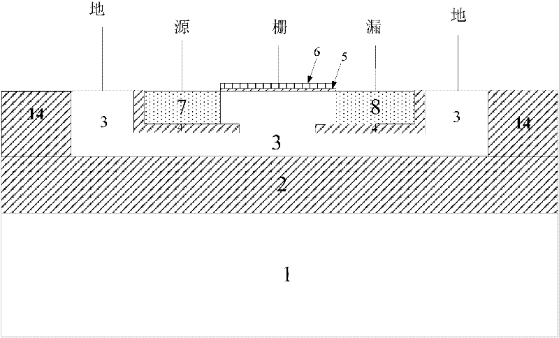
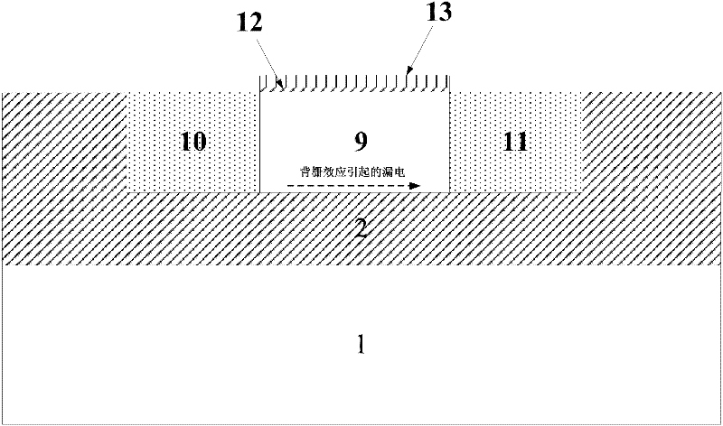
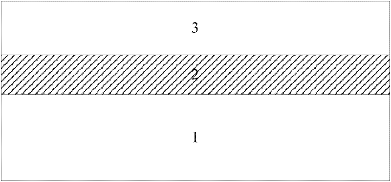
[0032] Such as figure 2 Shown: is the MOS device structure of the existing SOI process; the buried oxide layer 2 is set on the substrate 1, and the MOS device structure is formed in the buried oxide layer 2; wherein, the body region 9 of the MOS device is located at the center of the buried oxide layer 2 A device gate oxide layer 12 is provided on the body region 9, and a device polysilicon gate 13 is provided on the device gate oxide layer 12, and the gate terminal of the MOS device is formed by the device polysilicon gate 13 and the device gate oxide layer 12. A device source region 10 and a device drain region 11 are respectively formed on both sides of the body region 9 . The above-mentioned structure, under the influence of the total dose effect, will cause the back gate effect, resulting in the existence of leakage current between the source and the dra...
PUM
 Abstract
Description
Claims
Application Information