

Resistance type gas sensor with two support suspension beams and six-layer structure, and method thereof
A gas sensor and resistive technology, which is applied to resistive gas sensors with a six-layer structure of two-support cantilever beams and the field, can solve the problems of expensive process equipment, strict environmental conditions, and high cost, and achieve improved temperature uniformity and high mechanical strength. , the effect of low cost
- Summary
- Abstract
- Description
- Claims
- Application Information
AI Technical Summary
Problems solved by technology
Method used
Image

Examples
Embodiment 1
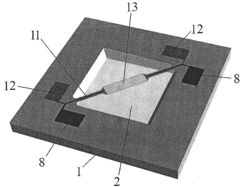
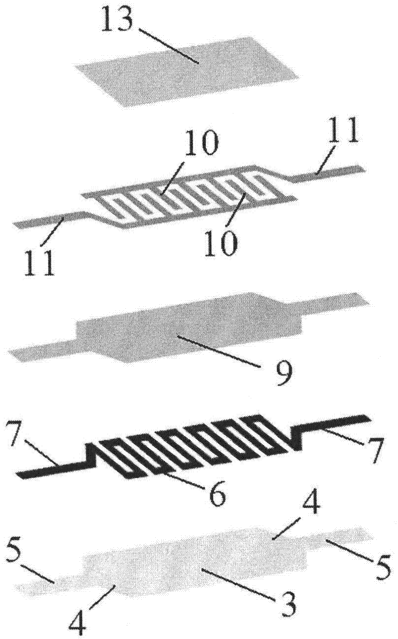
[0039] The structure schematic diagram of this embodiment sees figure 1 As shown, the specific production method is as follows:
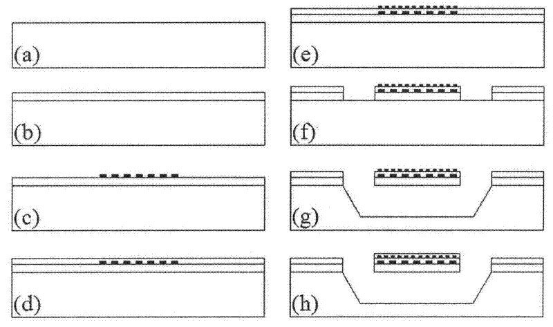
[0040] 1. Select the substrate. A 4-inch double-sided polished silicon wafer with an N-type (100) surface is selected as a substrate, the resistivity is 3-8Ω·cm, the thickness of the silicon wafer is 350±10 microns, and the angle error of trimming is <1%.
[0041] 2. Make a composite film. A single-layer composite film is used to sequentially grow a layer of silicon oxide with a thickness of 0.5 microns and a layer of silicon nitride with a thickness of 0.3 microns by means of low-pressure chemical vapor deposition (LPCVD).
[0042] 3. Make heating resistance wire, power supply lead wire and power supply electrode. Manufactured using a lift-off process. Thin photolithography (photoresist thickness is 2.0 microns) defines the pattern of heating resistance wire, power supply lead and power supply electrode, and then sputters a layer of 0.2 micron ...
Embodiment 2
[0049] The structure schematic diagram of this embodiment sees Figure 4 As shown, the specific production method is as follows:
[0050] 1. Select the substrate. A 4-inch double-sided polished silicon wafer with a P-type (100) surface is selected as the substrate, the resistivity is 3-8Ω·cm, the thickness of the silicon wafer is 350±10 microns, and the angle error of the edge trimming is less than 1%.
[0051] 2. Make a composite film. Using a single-layer composite film, a layer of silicon oxide with a thickness of 0.4 microns and a layer of silicon nitride with a thickness of 0.6 microns are sequentially grown by plasma enhanced chemical vapor deposition (PECVD).
[0052] 3. Make heating resistance wire, power supply lead wire and power supply electrode. Manufactured by wet etching process. First sputter a layer of titanium platinum with a thickness of 0.2 microns, then perform thin photolithography (the thickness of the photoresist is 1.8 microns) to define the pattern...
Embodiment 3
[0059] The structure schematic diagram of this embodiment sees Figure 5 As shown, the specific production method is as follows:
[0060] 1. Select the substrate. A 4-inch double-sided polished silicon wafer with a P-type (111) surface is selected as the substrate, the resistivity is 3-8Ω·cm, the thickness of the silicon wafer is 350±10 microns, and the angle error of the edge trimming is less than 1%.
[0061] 2. Make a composite film. Using a multi-layer composite film, a layer of silicon oxide with a thickness of 0.2 microns and a layer of silicon nitride with a thickness of 0.2 microns are sequentially deposited by low-pressure chemical vapor deposition (LPCVD), and then plasma-enhanced chemical vapor deposition (PECVD) A method of depositing a layer of silicon oxide with a thickness of 0.2 microns and a layer of silicon nitride with a thickness of 0.2 microns in sequence.
[0062] 3. Make heating resistance wire, power supply lead wire and power supply electrode. Manu...
PUM
| Property | Measurement | Unit |
|---|---|---|
| electrical resistivity | aaaaa | aaaaa |
| thickness | aaaaa | aaaaa |
Abstract
Description
Claims
Application Information