

Passivation dielectric film for solar cell
A technology for solar cells and dielectric films, applied in the field of solar cells, can solve the problems of loss of passivation effect, rapid crystallization of amorphous silicon films, and inability to use solar cells for production, to achieve enhanced passivation effect, good control, and improved photoelectric conversion. performance effect
- Summary
- Abstract
- Description
- Claims
- Application Information
AI Technical Summary
Problems solved by technology
Method used
Image

Examples
Embodiment 1
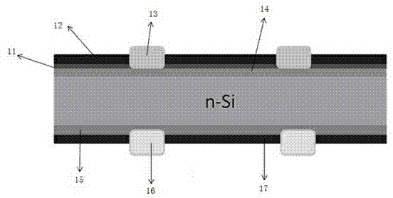
[0033] This example illustrates the application of laminated films on common n-type solar cells (the cross-sectional view of the cell is shown in figure 1 ), at this time the laminated film plays the role of passivation and optical anti-reflection at the same time. Specific steps are as follows:
[0034] A. Select a lightly doped n-type single crystal silicon wafer with a resistivity of 0.1~10 Ω·cm, place it in a texturing tank, and place it in a deionized aqueous solution of sodium hydroxide with a weight percentage of 0.5~5%. , the surface texture is carried out at a temperature of 75-90°C to form a suede structure;
[0035] B. Clean the surface of the silicon wafer with a chemical solution, the chemical solution is hydrofluoric acid, the concentration is 5-50%, the cleaning time is 0.5-60 minutes, and the temperature is 5-90°C;
[0036] C. After cleaning the above textured sheet, place it in a furnace tube at 700~1000°C for boron (B) diffusion to prepare a p-type emitter....
Embodiment 2
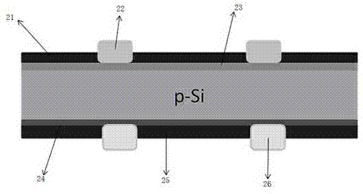
[0051] This embodiment illustrates the application of the laminated film structure on p-type silicon solar cells (see figure 2 ), mainly used for passivation of the backlight surface of the battery, the specific steps are as follows:
[0052] A. Select a lightly doped p-type single crystal silicon wafer with a resistivity of 0.1~10 Ω·cm, place the silicon wafer substrate in a texturing tank to remove the damaged layer and prepare the textured surface. The weight percentage is 0.5 In ~5% sodium hydroxide deionized aqueous solution, the surface texture is carried out at a temperature of 75~90°C to form a suede structure;
[0053] B. Clean the surface of the silicon wafer with a chemical solution, the chemical solution is hydrofluoric acid, the concentration is 5-50%, the cleaning time is 0.5-60 minutes, and the temperature is 5-90°C;
[0054] C. Place the silicon wafer in a furnace tube at 800-1000°C for phosphorus (P) diffusion, and form an n-type diffusion layer on the surfa...
Embodiment 3
[0064] This example illustrates that the laminated film structure is used in the production of p-type silicon solar cells to passivate the back surface of the cell and enhance the reflection of the unabsorbed solar long-wave photons on the back of the cell, thereby improving the photoelectric conversion efficiency of the cell . Specific steps are as follows:
[0065] A. Select a lightly doped p-type single crystal silicon wafer with a resistivity of 0.1~10 Ω·cm, place the silicon wafer substrate in a texturing tank to remove the damaged layer and prepare the textured surface. The weight percentage is 0.5 In ~5% sodium hydroxide deionized aqueous solution, the surface texture is carried out at a temperature of 75~90°C to form a suede structure;
[0066] B, the surface of the silicon chip is cleaned with a chemical solution, the chemical solution is a mixed solution of hydrofluoric acid and hydrochloric acid, wherein the ratio of hydrofluoric acid to hydrochloric acid is 1:1, a...
PUM
| Property | Measurement | Unit |
|---|---|---|
| thickness | aaaaa | aaaaa |
| thickness | aaaaa | aaaaa |
| thickness | aaaaa | aaaaa |
Abstract
Description
Claims
Application Information