P-type electric-conducting Sb mixed SnO2 film and stannic oxide homogeneous pn junction containing film and preparation methods thereof

A pn junction and tin oxide technology, which is applied in cable/conductor manufacturing, semiconductor/solid-state device manufacturing, circuits, etc., can solve the problems of difficult thickness control, poor film compactness and uniformity, and achieve easy control of process conditions and mature technology Effect

Inactive Publication Date: 2012-07-18
WUHAN UNIV OF TECH
View PDF1 Cites 16 Cited by
  • Summary
  • Abstract
  • Description
  • Claims
  • Application Information

AI Technical Summary

Problems solved by technology

When using the sol-gel method to deposit thin films on glass substrates, there are problems such a

Method used


Image

  • P-type electric-conducting Sb mixed SnO2 film and stannic oxide homogeneous pn junction containing film and preparation methods thereof
  • P-type electric-conducting Sb mixed SnO2 film and stannic oxide homogeneous pn junction containing film and preparation methods thereof
  • P-type electric-conducting Sb mixed SnO2 film and stannic oxide homogeneous pn junction containing film and preparation methods thereof

Examples


Embodiment 1

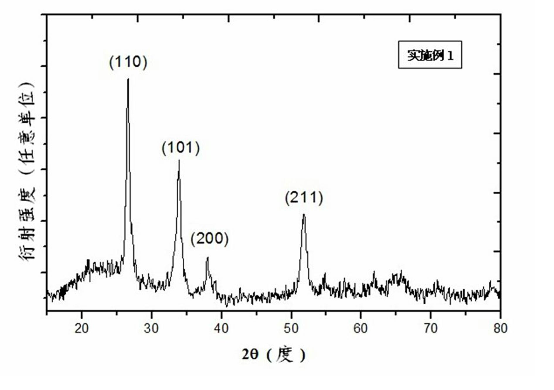
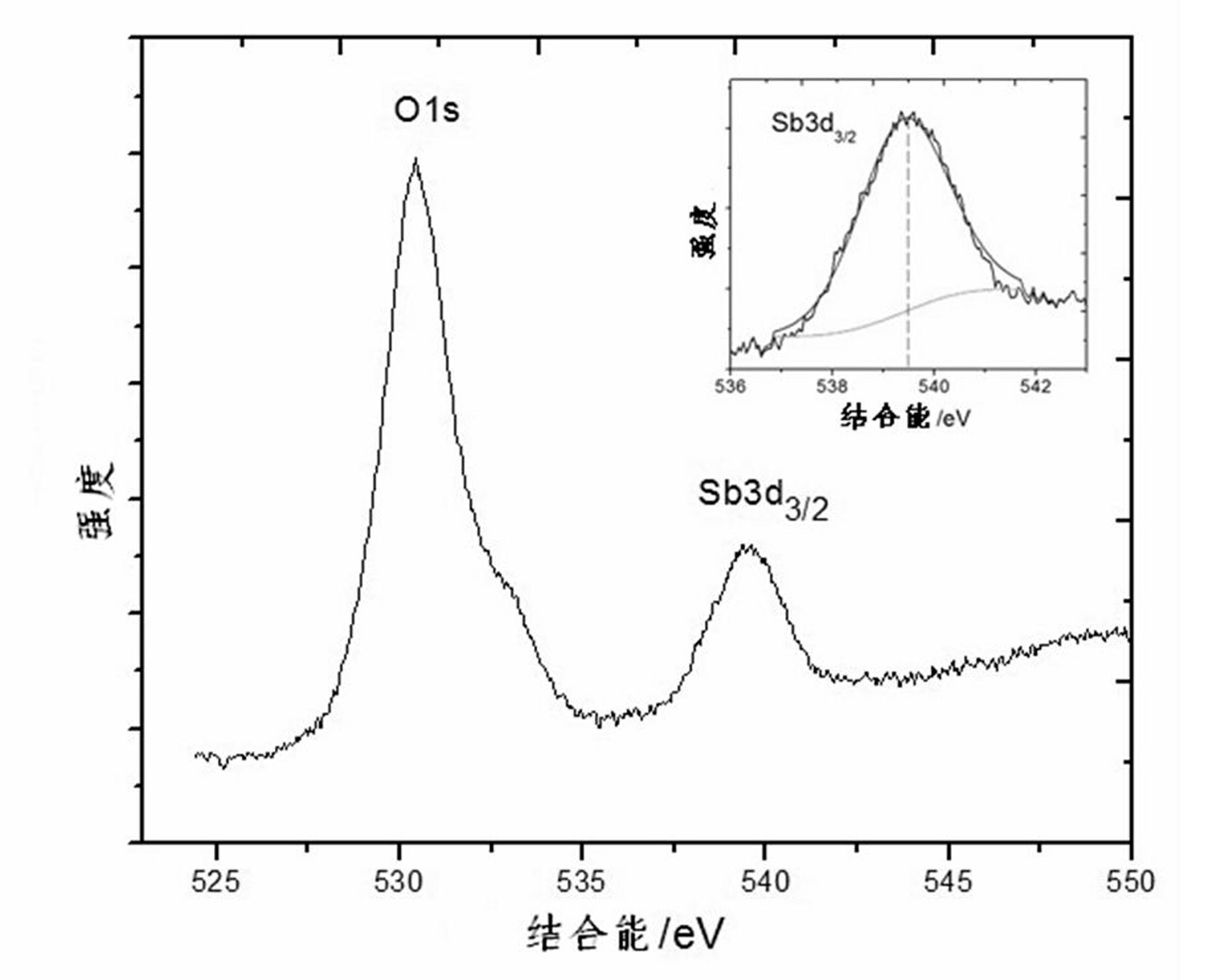
[0034] 1) Weigh SnO with purity ≧99.9% 2 and Sb 2 o 3 Powder, wherein the atomic ratio of Sb / (Sb+Sn) is 33:100, pour the above powder into a ball mill jar equipped with agate balls and add absolute ethanol for wet milling, the ball milling time is 5 hours, so that the powder can be mixed better Uniform and to some extent refined. Then the ground raw materials were dried in a drying oven at a temperature of 100° C. for 10 hours. Grind the dried raw materials in an agate grinder, and then use a mold to press the raw materials into shape. The molded body is subjected to cold isostatic pressing at 200 MPa, and finally placed in a sintering furnace, heated to 1250 °C at a rate of 3 °C per minute, kept for 5 hours, and naturally cooled to obtain p-type Sb-doped SnO 2 ceramic target;

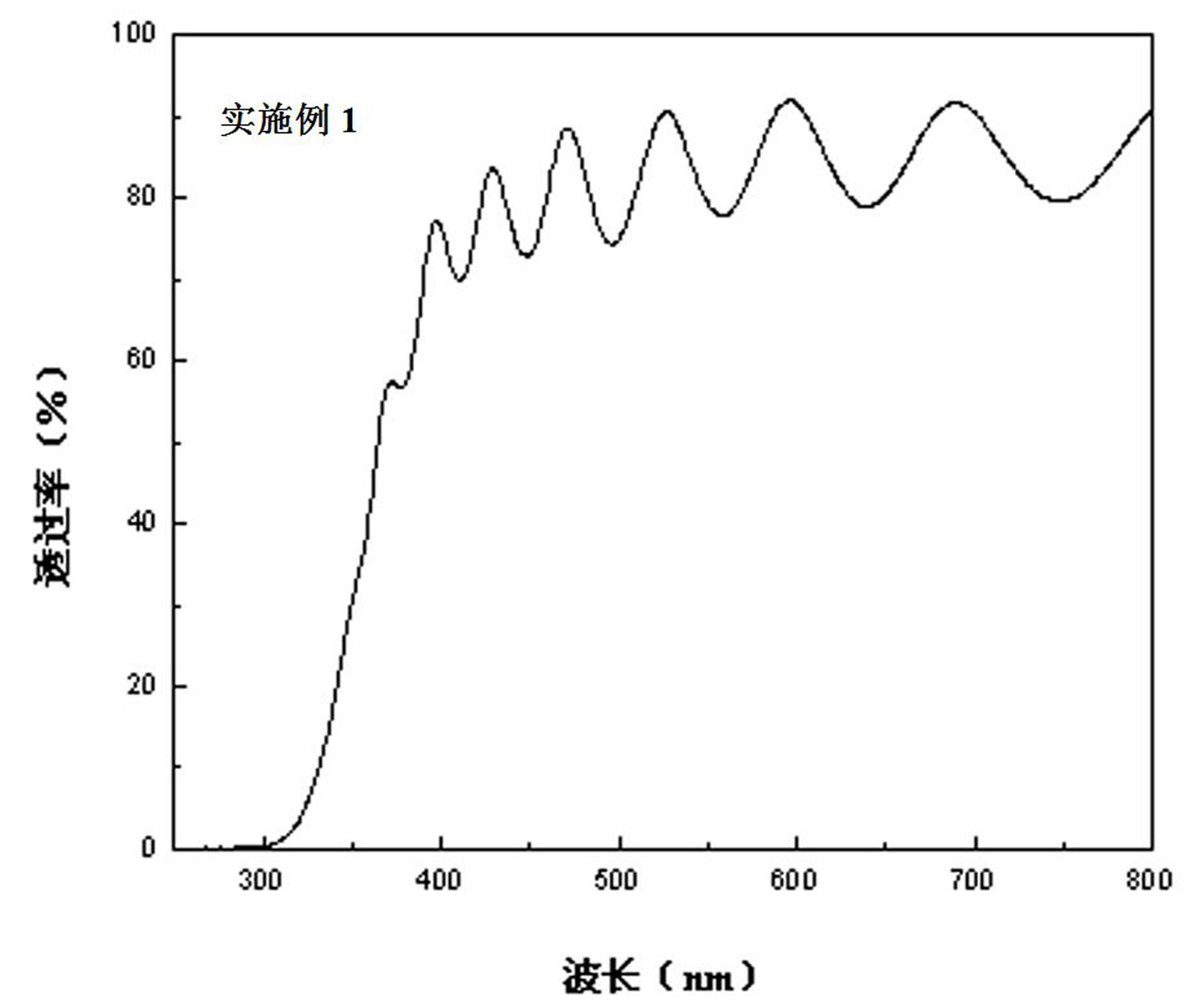
[0035] 2) Using the p-type Sb-doped SnO made in step 1) 2 Ceramic target, using magnetron sputtering method, with quartz glass as substrate, substrate temperature 200°C, high-purity argon as work...

Embodiment 2

[0038] 1) Weigh SnO with purity ≧99.9% 2 and Sb 2 o 3 Powder, wherein the atomic ratio of Sb / (Sb+Sn) is 18:100, pour the above powder into a ball mill jar equipped with agate balls and add absolute ethanol for wet milling, the ball milling time is 5 hours, so that the powder can be mixed better Uniform and to some extent refined. Then the ground raw materials were dried in a drying oven at a temperature of 100° C. for 10 hours. Grind the dried raw materials in an agate grinder, and then use a mold to press the raw materials into shape. The molded body is subjected to cold isostatic pressing at 200 MPa, and finally placed in a sintering furnace, heated to 1250 °C at a rate of 3 °C per minute, kept for 5 hours, and naturally cooled to obtain p-type Sb-doped SnO 2 ceramic targets.

[0039] 2) Using the Sb-doped SnO made in step 1) 2 Ceramic target, using magnetron sputtering method, using single crystal Si (100) sheet as substrate, substrate temperature 250°C, high-purity a...

Embodiment 3

[0042] Adopt the p-type Sb doped SnO prepared on the quartz substrate obtained in embodiment 1 2 The thin film is used as the substrate, and the first layer of p-type Sb is doped with SnO by radio frequency magnetron sputtering method. 2 A second layer of n-type Sb-doped SnO is plated on the film 2 film. The specific method is as follows:

[0043] 1) n-type Sb doped SnO2 Preparation of ceramic target: Weighing SnO with purity ≧99.9% 2 and Sb 2 o 5 Powder, wherein the atomic ratio of Sb / (Sb+Sn) is 11:100, the above powder is mixed uniformly by ball milling, pressed into shape, and then sintered at 1250°C for 5h to obtain n-type Sb-doped SnO 2 ceramic target;

[0044] 2) Using the n-type Sb-doped SnO made in step 1) 2 Ceramic target material, utilizes magnetron sputtering method, is coated with p-type Sb doping SnO with the obtained in embodiment 1 2 thin-film quartz glass as the substrate, p-type Sb doped with SnO 2 A layer of n-type Sb-doped SnO was deposited on the f...


PUM

PropertyMeasurementUnit
Thicknessaaaaaaaaaa
Conductivityaaaaaaaaaa
Hall mobilityaaaaaaaaaa

Abstract

The invention relates to a p-type electric-conducting Sb mixed SnO2 film and a stannic oxide homogeneous pn junction containing film and preparation methods thereof. The p-type electric-conducting Sb mixed SnO2 film is prepared by adopting Sb mixed SnO2 ceramic target on single crystal and quartz glass in a magnetron sputtering method. The stannic oxide homogeneous pn junction is prepared by sputtering and depositing an n-type Sb mixed SnO2 film on the p-type electric-conducting Sb mixed SnO2 film. The p-type electric-conducting Sb mixed SnO2 film is stable in electric conductivity, has high hole concentration, hole mobility and specific conductance and has high transparency in visible light, wherein hole concentration is as high as 1020cm-3 order of magnitudes, specific conductance is 60S.cm-1, and hole mobility is as high as 2-30cm<2>V-1s-1. The preparation methods are simple in process and good in repeatability, can be industrialized easily, and the prepared homogeneous stannic oxide based transparent pn junction has volt-ampere curve characteristics of wide bandgap semiconductor pn junction.

Description

technical field [0001] The invention belongs to the technical field of transparent conductive materials, in particular to a p-type conductive Sb-doped SnO with high electrical conductivity, high hole concentration, high mobility, and high visible light transmittance. 2 Thin film and corresponding tin oxide homogeneous pn junction and preparation method thereof. Background technique [0002] Transparent conductive oxide (TCO) films and their corresponding transparent pn junction light-emitting diodes (LEDs), lasers (LDs), energy-saving white light lighting LEDs, gas sensors, solar cells, liquid crystal displays, smart windows, etc. The field has broad application prospects. Although various high-performance n-type TCO materials have been obtained so far, such as Sn-doped In 2 o 3 (ITO), Al-doped ZnO (AZO), etc., but due to the self-compensation effect in oxide semiconductors, it is difficult to obtain high-performance p-type TCO materials through doping. Due to the presen...

Claims


Application Information

Patent Timeline
IPC IPC(8): C23C14/35C23C14/06H01L21/363H01B13/00
CPCC23C14/086C04B35/00C23C14/35H01L21/02579H01L21/02565H01L21/02483H01L21/02422C23C14/3414H01L21/02631H01L21/02381C04B35/457C04B2235/3293C04B2235/3294C04B2235/6562C04B2235/6567
Inventor 赵修建倪佳苗耿硕麒刘启明
Owner WUHAN UNIV OF TECH
Why Eureka
Try Eureka