

Field effect gas sensor taking air gap as insulation layer and preparation method thereof
A gas sensor and air gap technology, applied in the field of sensing, can solve the problem of improving the sensitivity of field effect gas sensors, limiting field effect one-dimensional micro-nano single-crystal gas sensors, slowing down the development of device miniaturization and nanometerization, etc. problems, to avoid the tip effect, improve device performance, and ensure stability and repeatability
- Summary
- Abstract
- Description
- Claims
- Application Information
AI Technical Summary
Problems solved by technology
Method used
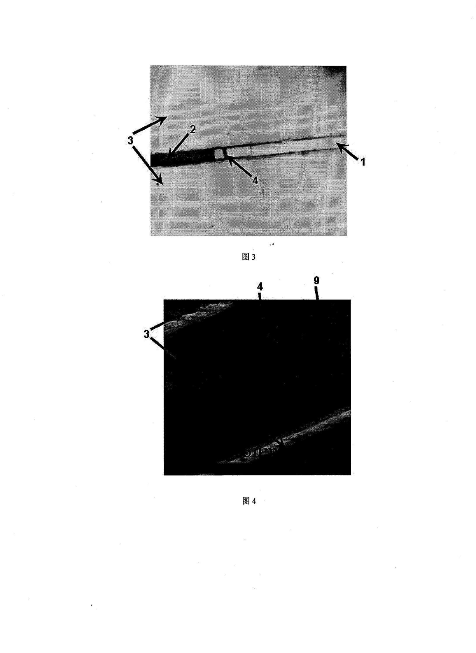
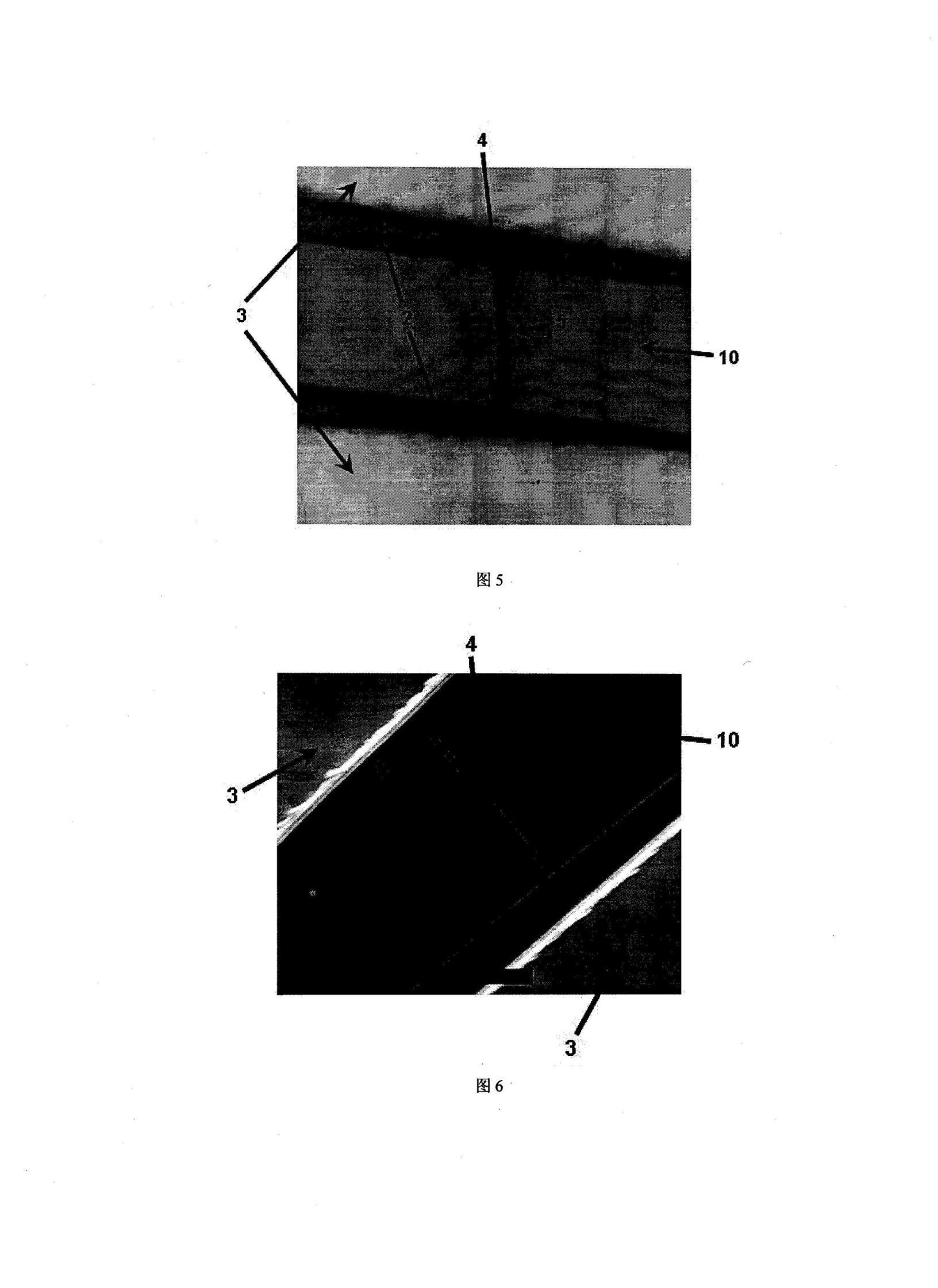
Image

Examples
Embodiment 1
[0033] Embodiment 1, Preparation method 1 of a field effect transistor gas sensor with an air gap as an insulating layer:
[0034] Device Fabrication Process The air gap grooves are prepared by spin-coating PMMA on the surface of the substrate combined with electron beam exposure technology. The source and drain electrodes are prepared by using the gold sheet film electrode method or photolithography method. The micro-nano single crystal is placed above the air gap by mechanical movement.
[0035] The field-effect gas sensor provided by the present invention to manufacture an air gap as an insulating layer comprises the following steps:
[0036] (1) Clean the glass substrate with a standard silicon wafer cleaning process, and then use photolithography to prepare Ti / Au (10nm / 20nm) electrodes as the gate of the device;
[0037](2) The anisole solvent is equipped with PMMA with a mass volume ratio of 6%, and the prepared PMMA solution is dripped on the glass sheet, and spin-c...
Embodiment 2
[0043] Embodiment 2, Preparation method 2 of field effect transistor gas sensor with air gap as insulating layer:
[0044] Proceed as follows:
[0045] (1) Clean the heavily doped Si as the gate of the device with a standard silicon wafer cleaning process;
[0046] (2) Step (2) in Example 1 is used to spin-coat two layers of PMMA on Si to obtain 510nm PMMA.
[0047] (3) A groove with a width of 10 microns and a smooth bottom is prepared on the gate by electron beam exposure technology, and heavily doped Si is used as the gate. Both sides of the trench are used to support copper phthalocyanine nanobelts.
[0048] (4) As in step (4) in Example 1, the micro-nano crystals are mechanically moved to place a single copper phthalocyanine nanoribbon above the air gap, and the width of the micro-nano single crystal is 350nm.
[0049] (5) Step (5) in Example 1 is used to prepare source-drain electrodes.
[0050] (6) The air gap between the semiconductor and the bottom of the trenc...
Embodiment 3
[0053] Embodiment 3, Application of Field Effect Transistor Gas Sensor with Air Gap as Insulator (Taking Copper Phthalocyanine Nanoribbons as an Example)
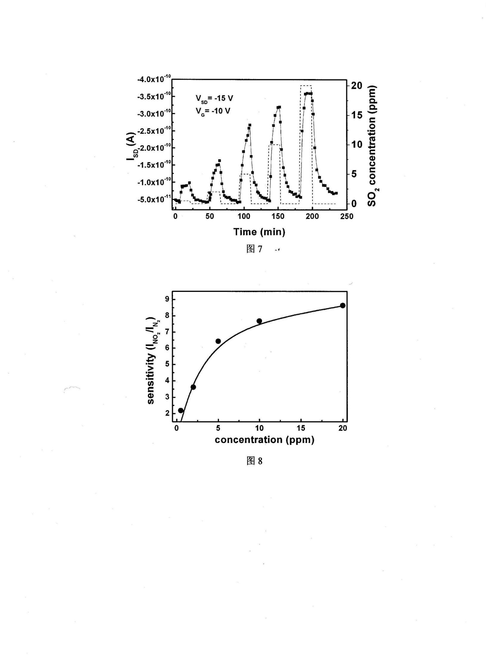
[0054] Device pair SO 2 Gas-sensitive characteristics:
[0055] Connect the finished device to the self-made stainless steel gas-sensing test system by using a gold wire ball welding machine. The air pressure was maintained at one atmosphere during the test. The gas flow rate was 500 sccm. In the test we chose the gate voltage as V G =-10 V, the source-drain voltage is V SD =-15V. The gas concentration is controlled by a mass flow meter, and the balance gas is N 2 . Measured gas SO 2 The concentration of the gas is 0.5-20ppm, and the measured gas flow time is 15min, and then the high-purity N 2 The access time was set at 30 min. Test device against SO 2 Gas sensitivity characteristics and sensitivity.
[0056] Figure 7 and Figure 8 Field-effect gas sensors prepared for copper phthalocyanine single nanobelt...
PUM
 Abstract
Description
Claims
Application Information