

Rubber conductive particle and preparation method thereof
A technology of conductive particles and rubber, which is applied in the field of electrical conductors, can solve problems such as high cost, high failure rate, and complex structure, and achieve the effects of less pollutants, firm combination, and wide application
- Summary
- Abstract
- Description
- Claims
- Application Information
AI Technical Summary
Problems solved by technology
Method used
Image

Examples
Embodiment 1
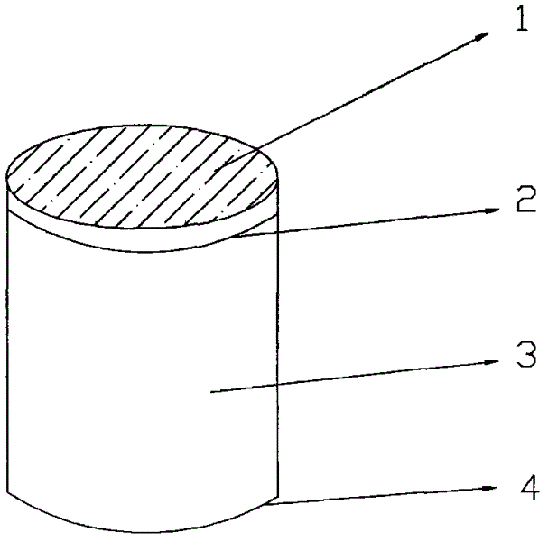
[0031] The polyurethane rubber substrate 3 sheet is prepared by molding, and the upper surface 2 of the rubber substrate is cleaned with argon plasma in a coating machine, and then, the rubber substrate of this sheet is coated by vacuum sputtering. One layer of 316 stainless steel metal coating with a thickness of 5 μm is sputtered on the upper surface 2 of the material. This polyurethane sheet deposited with one layer of stainless steel metal coating was punched out into small cylindrical particles with a diameter of 3 mm. The surface conductive small particles are used as the conductive contact element of the circuit board of the substrate, and the lower surface 4 of the rubber substrate is compounded with the silicone rubber printed with numbers, so that the keys on the mobile phone can be prepared. The preparation cost of such conductive particles is relatively low.
Embodiment 2
[0033] The butyl rubber substrate 3 sheet is obtained by extrusion molding, and the butyl rubber substrate 3 contains pigments, fillers, antiaging agents, toughening agents, plasticizers, antistatic agents, crosslinking agents or coupling agents. coupling agent; clean the rubber base material upper surface 2 of butyl rubber with corona treatment, and then first plate a copper film with a thickness of 10 μm on the rubber base material upper surface 2 by vacuum evaporation coating, and then A gold film with a thickness of 1 μm was plated by a vacuum ion plating process. This rubber substrate 3 sheet with two layers of metal coating 1 is cut into polygonal granules with a diameter of 6 mm. The surface conductive small particles are used as the conductive contact element of the circuit board of the substrate, and the lower surface 4 of the rubber substrate is compounded with the silicone rubber printed with numbers, so that the buttons on the cordless telephone can be prepared. T...
Embodiment 3
[0035] The silicone rubber substrate 3 sheet is prepared by calendering, and the silicone rubber substrate 3 contains pigments, fillers, antiaging agents, toughening agents, plasticizers, antistatic agents, crosslinking agents or coupling agents; The upper surface 2 of the rubber substrate has a strip-shaped geometric pattern, and the upper surface 2 of the silicone rubber substrate is treated by spraying a coupling agent. An aluminum film with a thickness of 0.05mm is plated on the top, and then a nickel film with a thickness of 0.01mm is plated with an electroless plating process. This rubber substrate 3 sheet with two layers of metal coating 1 is laser cut into small elliptical particles with a diameter of 10 mm. The surface conductive small particles are used as the conductive contact element of the circuit board of the substrate, and the lower surface 4 of the rubber substrate is compounded with the silicone rubber printed with letters, so that the keys of the computer ca...
PUM
| Property | Measurement | Unit |
|---|---|---|
| Total thickness | aaaaa | aaaaa |
| Thickness | aaaaa | aaaaa |
| Thickness | aaaaa | aaaaa |
Abstract
Description
Claims
Application Information