High-threshold voltage gallium nitride enhanced transistor structure and preparation method thereof

A high-threshold voltage, gallium nitride technology, used in semiconductor/solid-state device manufacturing, circuits, electrical components, etc., can solve the problem of poor performance of GaN integrated circuits, degradation of device electrical performance, and difficulty in accurately controlling the thickness of the AlGaN barrier layer in the gate region. and other problems, to achieve the effect of wide device operating voltage range, high source-drain saturation current density, and good controllability of the preparation process.

A high-threshold voltage, gallium nitride technology, used in semiconductor/solid-state device manufacturing, circuits, electrical components, etc., can solve the problem of poor performance of GaN integrated circuits, degradation of device electrical performance, and difficulty in accurately controlling the thickness of the AlGaN barrier layer in the gate region. and other problems, to achieve the effect of wide device operating voltage range, high source-drain saturation current density, and good controllability of the preparation process.

CN102709322AInactive Publication Date: 2012-10-03UNIV OF ELECTRONICS SCI & TECH OF CHINA

Image

  • High-threshold voltage gallium nitride enhanced transistor structure and preparation method thereof
  • High-threshold voltage gallium nitride enhanced transistor structure and preparation method thereof
  • High-threshold voltage gallium nitride enhanced transistor structure and preparation method thereof

Examples


Embodiment Construction

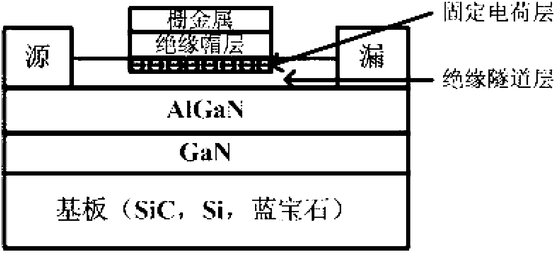
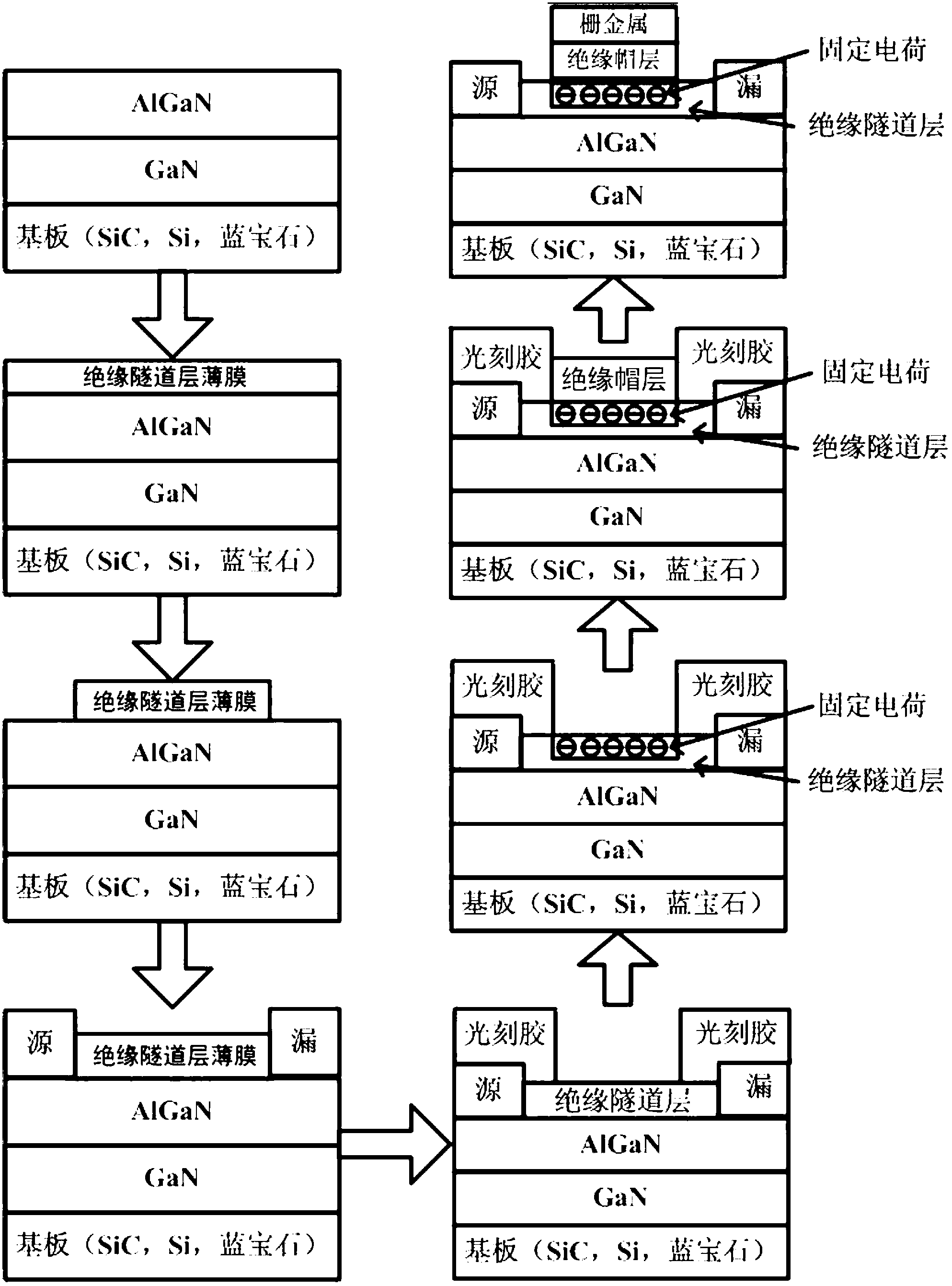
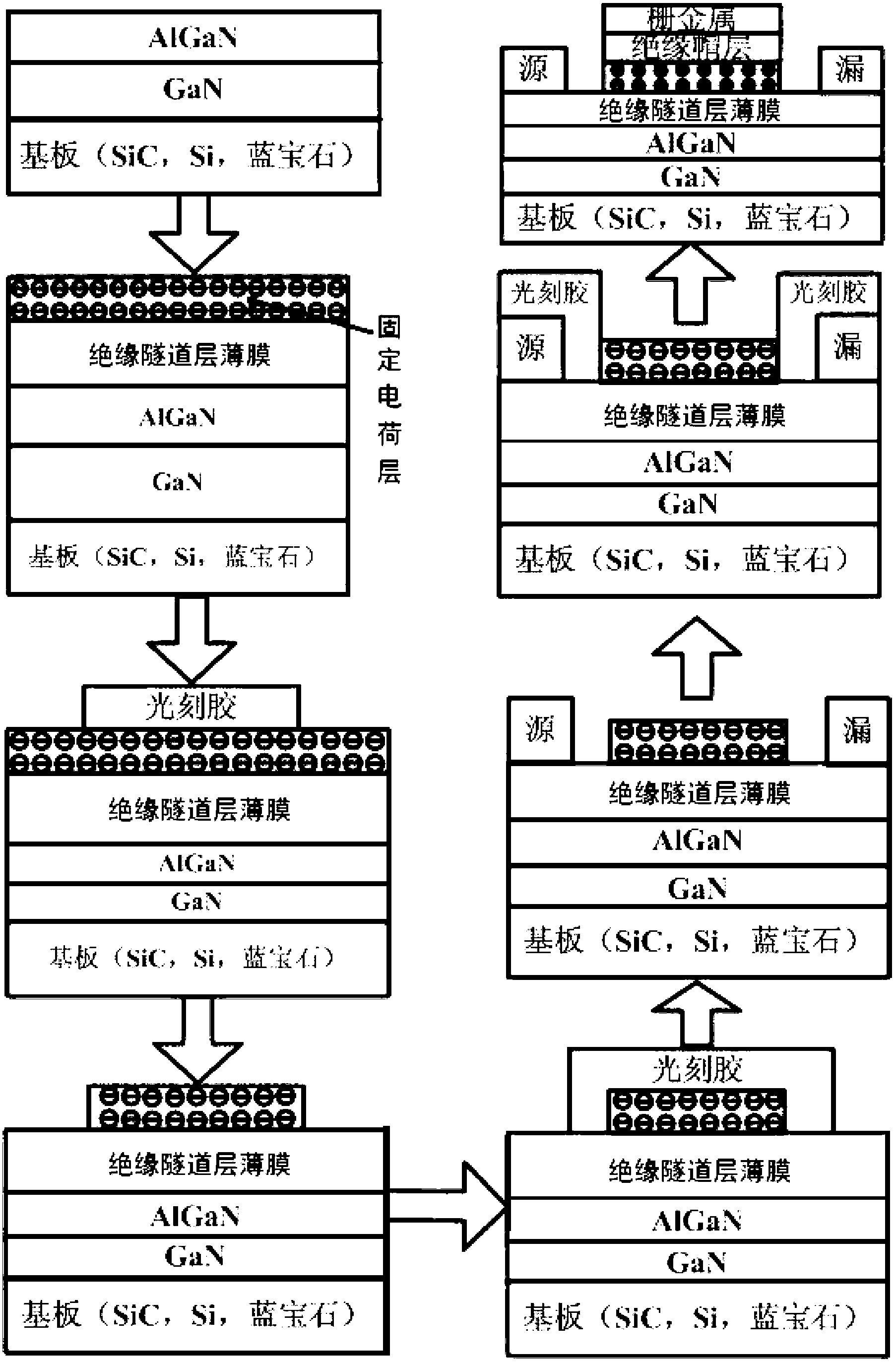
[0032] The schematic diagram of the basic structure of the enhanced GaN HEMT device of the present invention is as figure 1 As shown, it belongs to metal-insulator-semiconductor (MIS) field effect transistor. Compared with the common MIS structure GaN field effect transistor, the characteristics of the MIS structure GaN field effect transistor of the present invention are: the insulating gate dielectric includes an insulating cap layer, The three parts of the fixed negative charge layer and the insulating tunnel layer deplete the two-dimensional electron gas in the gate region by the charge of the fixed negative charge layer to achieve a threshold voltage greater than zero, and then further increase the threshold voltage of the device by introducing an insulating cap layer, thereby manufacturing GaN-enhanced high electron mobility transistors with higher thresholds, in which the insulating gate dielectric is mainly made of Al 2 o 3 , SiO 2 , HfO 2 , HfTiO, ZrO 2 、SiN x , ...


PUM


Abstract

The invention provides a high-threshold voltage gallium nitride enhanced transistor structure and a preparation method thereof and relates to semiconductor technology. The high-threshold voltage gallium nitride enhanced transistor structure comprises a substrate, a GaN layer, an AlGaN layer and an insulating gate dielectric layer from bottom to top and is characterized in that the insulating gate dielectric layer comprises an insulating tunnel layer, a fixed charge layer and an insulating cap layer, wherein the fixed charge layer is arranged above the insulating tunnel layer or is embedded at the upper part of the insulating tunnel layer; the insulating cap layer is arranged above the fixed charge layer; and gate metal is arranged above the insulating cap layer. The high-threshold voltage gallium nitride enhanced transistor structure has the beneficial effects that compared with other technology for manufacturing an enhanced GaN field effect transistor, the controllability of the preparation process is good, and the performance repeatability of researched and developed devices is good; and a researched and developed GaN MlSHEMT device has the advantages of good performance, large threshold voltage, large biggest source leakage saturation current density, small gate current leakage and wide operating voltage range, and the research and development demands of a GaN integrated circuit can be fully satisfied.

Description

technical field [0001] The present invention relates to semiconductor technology. Background technique [0002] Compared with high electron mobility transistors (HEMTs) based on AlGaAs / GaAs (AlGaAs / GaAs) heterojunctions, HEMT devices based on AlGaN / GaN (AlGaN / GaN) heterojunctions have the following advantages: [0003] (1) The two-dimensional electron gas (2DEG) concentration at the AlGaN / GaN heterojunction interface is relatively high (up to 1013cm-2), which is nearly an order of magnitude higher than the 2DEG concentration at the AlGaAs / GaAs heterojunction interface. Therefore, based on AlGaN / GaN heterojunction HEMT will have higher output power density. As a mass-produced product, the power density of HEMT devices based on AlGaN / GaN heterojunction has reached more than 10W / mm, which is nearly 20 times higher than that of GaAs-based HEMT devices. [0004] (2) Since GaN is a wide bandgap semiconductor, its operating temperature is high and can work normally above 500Β°C, w...

Claims


Application Information

Patent Timeline
03 Oct 2012
Publication
CN102709322A
IPC
H01L29/778; H01L21/335
Inventors
εˆ˜ε…΄ι’Š; ι™ˆθΆ