

SOI (Silicon On Insulator)-BJT (Bipolar Junction Transistor) Bi CMOS (Complementary Metal-Oxide-Semiconductor) integrated device with strain SiGe clip-shaped channel and preparation method thereof
An integrated device and channel direction technology, which is applied in semiconductor/solid-state device manufacturing, electric solid-state devices, semiconductor devices, etc., can solve problems such as threshold voltage drift, large influence, oxide layer breakdown, etc. Effect of mobility and performance improvement
- Summary
- Abstract
- Description
- Claims
- Application Information
AI Technical Summary
Problems solved by technology
Method used
Image

Examples
Embodiment 1
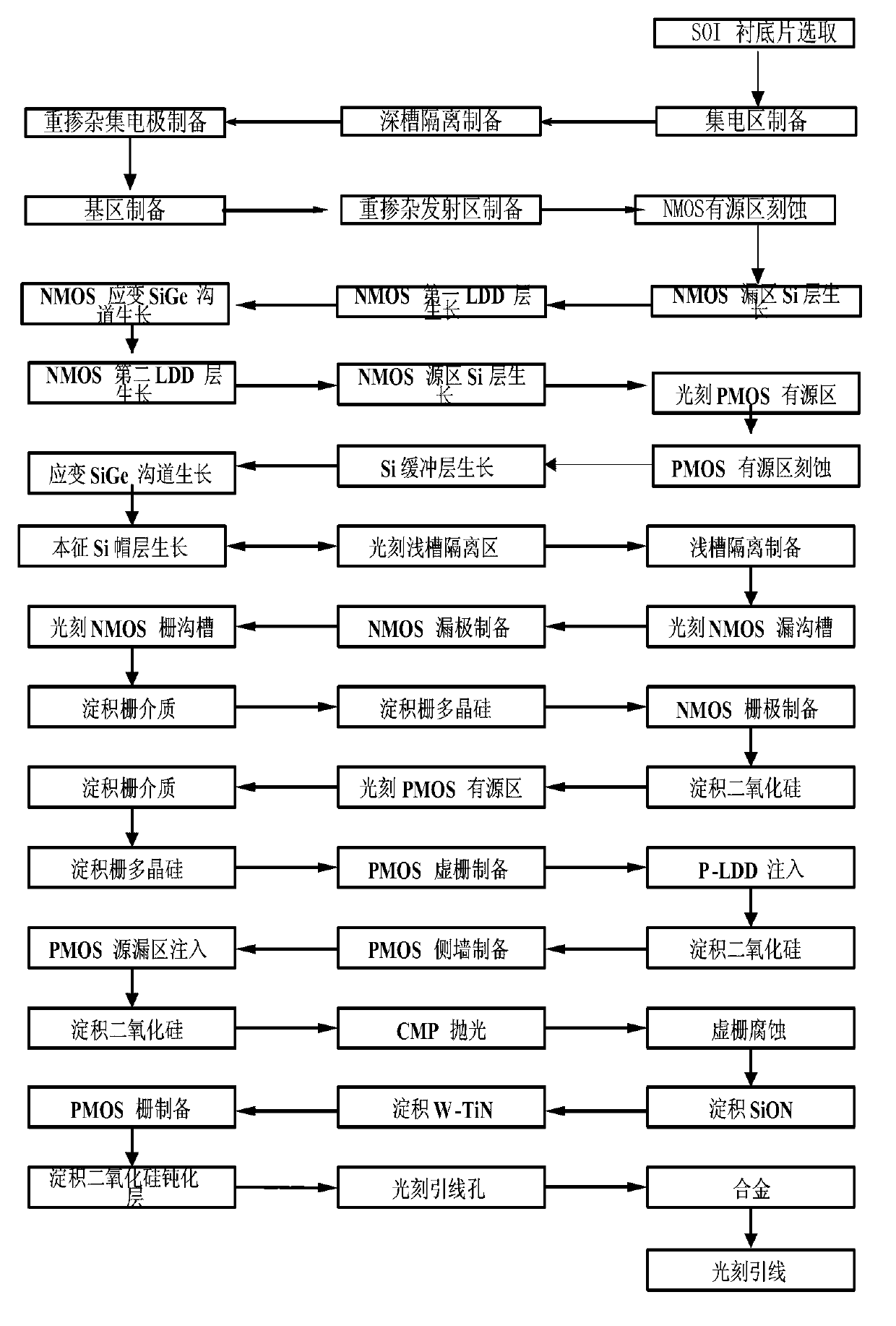
[0112] Embodiment 1: Prepare the SOI BJT, the strained SiGe back channel BiCMOS integrated device and the circuit with the conductive channel of 45nm, the specific steps are as follows:
[0113] Step 1, epitaxial growth.
[0114] (1a) Select the SOI substrate, the support material of the lower layer of the substrate is Si, and the middle layer is SiO 2 , with a thickness of 150nm, and the upper material is doped with a concentration of 1×10 16 cm -3 N-type Si with a thickness of 100nm;
[0115] (1b) Thermally oxidize a layer of SiO with a thickness of 300nm on the substrate surface 2 layer.
[0116] Step 2, isolation area preparation.
[0117] (2a) Epitaxially grow a layer with a doping concentration of 1×10 on the SOI substrate 16 cm -3 A Si layer with a thickness of 0.3 μm acts as a collector area;
[0118] (2b) Thermally oxidize a layer of SiO with a thickness of 200nm on the substrate surface 2 layer;
[0119] (2c) In the photolithographic isolation area, a deep...
Embodiment 2
[0176] Embodiment 2: prepare SOI BJT, strained SiGe back-channel BiCMOS integrated device and circuit with conductive channel of 30nm, the specific steps are as follows:
[0177] Step 1, epitaxial growth.
[0178] (1a) Select the SOI substrate, the support material of the lower layer of the substrate is Si, and the middle layer is SiO 2 , with a thickness of 300nm, and the upper material is doped with a concentration of 5×10 16 cm -3 N-type Si with a thickness of 120nm;
[0179] (1b) Thermally oxidize a layer of SiO with a thickness of 400nm on the substrate surface 2 layer.
[0180] Step 2, isolation area preparation.
[0181] (2a) Epitaxial growth on SOI substrate with a doping concentration of 5×10 16 cm -3 A Si layer with a thickness of 0.5 μm acts as a collector area;
[0182] (2b) Thermally oxidize a layer of SiO with a thickness of 250nm on the substrate surface 2 layer;
[0183] (2c) In the photolithographic isolation area, a deep trench with a depth of 4 μm...
Embodiment 3
[0240] Embodiment 3: The SOI BJT, the strained SiGe back channel BiCMOS integrated device and the circuit with the conductive channel of 22nm are prepared, and the specific steps are as follows:
[0241] Step 1, epitaxial growth.
[0242] (1a) Select the SOI substrate, the support material of the lower layer of the substrate is Si, and the middle layer is SiO 2 , with a thickness of 400nm, and the upper material is doped with a concentration of 1×10 17 cm -3 N-type Si with a thickness of 150nm;
[0243] (1b) Thermally oxidize a layer of SiO with a thickness of 500nm on the surface of the substrate 2 layer.
[0244] Step 2, isolation area preparation.
[0245] (2a) Epitaxial growth on SOI substrate with a doping concentration of 1×10 17 cm -3 A Si layer with a thickness of 0.8 μm acts as a collector area;
[0246] (2b) Thermally oxidize a layer of SiO with a thickness of 300nm on the substrate surface 2 layer;
[0247] (2c) In the photolithographic isolation area, a ...
PUM
| Property | Measurement | Unit |
|---|---|---|
| Thickness | aaaaa | aaaaa |
| Thickness | aaaaa | aaaaa |
| Thickness | aaaaa | aaaaa |
Abstract
Description
Claims
Application Information