

Device and method for reinforcing electro-catalytic degradation of organic wastewater by using visible light
A technology for electrocatalytic degradation and organic wastewater, which is applied in energy wastewater treatment, light water/sewage treatment, oxidized water/sewage treatment, etc. It can solve the problems of complex types of organic matter, poor selective adsorption of photocatalysts, and low photocatalytic quantum efficiency. , to achieve the effect of improving energy transmission rate, realizing selective photocatalysis, and improving catalytic efficiency
- Summary
- Abstract
- Description
- Claims
- Application Information
AI Technical Summary
Problems solved by technology
Method used
Image


Examples
Embodiment 1
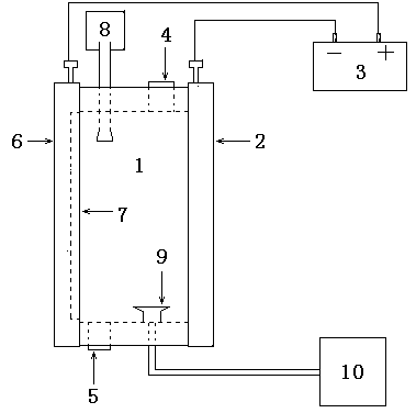
[0026] figure 1 It is a schematic structural diagram of the device for the visible light-enhanced electrocatalytic degradation of organic wastewater of the present invention. As shown in the figure, the device for visible light-enhanced electrocatalytic degradation of organic wastewater in this embodiment includes an organic wastewater container 1, a photoanode, a cathode 2 and a DC power supply 3. The organic wastewater container 1 is provided with a water inlet 4 and a water outlet 5, the photoanode and the cathode 2 are located in the organic wastewater container 1, and the photoanode includes a conductive substrate 6 and a silicon substrate mounted on the conductive substrate 6. sheet 7, the silicon sheet 7 is provided with a metal coating on one side close to the conductive substrate 6, and the other side is provided with a micron hole, the conductive substrate 6 of the photoanode is connected to the positive pole of the DC power supply 3, and the cathode 2 is connected to...
Embodiment 2
[0034] The difference between the visible light-enhanced electrocatalytic degradation device for organic wastewater of this embodiment and that of Embodiment 1 is that the metal coating on one side of the silicon wafer 7 is uniformly plated on the surface of the silicon wafer by vacuum ion plating, and the metal coating on the other side of the silicon wafer 7 The nanopores are prepared by electrochemical anodization method. The specific preparation process is: the silicon wafer is sandwiched in a single-sided anodization reactor with an O-ring design, and the volume ratio of 1:7:6 is poured into hydrofluoric acid, Mixed reaction solution of hydrogen peroxide and absolute ethanol, the platinum electrode is the counter electrode, forming a two-electrode electrochemical reaction system, the current density is 30mA / cm 2 , the anodic oxidation time is 3 minutes, and the pore diameter of the formed channel is about 20nm.
[0035] The method for degrading organic wastewater using th...
Embodiment 3
[0037] The difference between the visible light-enhanced electrocatalytic degradation device for organic wastewater of this embodiment and that of Embodiment 1 is that the metal coating on one side of the silicon wafer 7 is uniformly plated on the surface of the silicon wafer by vacuum ion plating, and the metal coating on the other side of the silicon wafer 7 The nanopores are prepared by electrochemical anodic oxidation method. The specific preparation process is as follows: the silicon wafer is sandwiched in a single-sided anodic oxidation reactor with an O-ring design, and the volume ratio of 1:10:6 is poured into hydrofluoric acid, Mixed reaction solution of hydrogen peroxide and absolute ethanol, the platinum electrode is the counter electrode, forming a two-electrode electrochemical reaction system, the current density is 40mA / cm 2 , the anodic oxidation time is 5 minutes, and the pore diameter of the formed channel is about 200nm.
[0038] The method for degrading orga...
PUM
| Property | Measurement | Unit |
|---|---|---|
| pore size | aaaaa | aaaaa |
Abstract
Description
Claims
Application Information