BiCMOS (Bipolar Complementary Metal Oxide Semiconductor) integrated device on basis of SOI (Silicon On Insulator) substrate and preparation method

A technology for integrated devices and substrates, applied in the field of BiCMOS integrated devices and preparations based on SOI substrates, can solve the problems of low carrier material mobility, confinement, and low mechanical strength of Si materials

Inactive Publication Date: 2015-07-22
XIDIAN UNIV
View PDF2 Cites 0 Cited by
  • Summary
  • Abstract
  • Description
  • Claims
  • Application Information

AI Technical Summary

Problems solved by technology

Although GaAs and InP-based compound devices have superior frequency characteristics, their preparation process is more complicated than Si process, high cost, difficult to prepare large-diameter single crystal, low mechanical strength, poor heat dissipation performance, incompatibility with Si process and lack of SiO 2 Such passivation layer and other factors limit its wide application and development.
[0007] Due to the low mobility of Si materials, the performance of integrated circuits manufactured by Si BiCMOS technology, especially the frequency performance, is greatly limited; for SiGe BiCMOS technology, although SiGe HBT is used for bipolar transistors, However, Si CMOS is still used for unipolar devices that restrict the improvement of the frequency characteristics of BiCMOS integrated circuits, so these limit the further improvement of the performance of BiCMOS integrated circuits

Method used


Image

  • BiCMOS (Bipolar Complementary Metal Oxide Semiconductor) integrated device on basis of SOI (Silicon On Insulator) substrate and preparation method

Examples


Embodiment 1

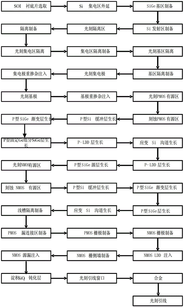
[0128] Embodiment 1: preparation channel length is the BiCMOS integrated device and circuit based on SOI substrate of 22nm, concrete steps are as follows:

[0129] Step 1, epitaxial growth.

[0130] (1a) Select the SOI substrate, the support material of the lower layer of the substrate is Si, and the middle layer is SiO 2 , with a thickness of 150nm, and the upper material is doped with a concentration of 1×10 16 cm -3 N-type Si with a thickness of 100nm;

[0131] (1b) Using chemical vapor deposition (CVD), grow a layer of N-type epitaxial Si layer with a thickness of 50nm on the upper Si material at 600°C, as the collector region, and the doping concentration of this layer is 1× 10 16 cm -3 ;

[0132] (1c) Using chemical vapor deposition (CVD), grow a SiGe layer with a thickness of 20nm on the substrate at 600°C. As the base region, the Ge composition of this layer is 15%, and the doping concentration is 5×10 18 cm -3 ;

[0133] (1d) Using the method of chemical vap...

Embodiment 2

[0200] Embodiment 2: preparation channel length is the BiCMOS integrated device and circuit based on SOI substrate of 30nm, concrete steps are as follows:

[0201] Step 1, epitaxial growth.

[0202] (1a) Select the SOI substrate, the support material of the lower layer of the substrate is Si, and the middle layer is SiO 2 , with a thickness of 300nm, and the upper material is doped with a concentration of 5×10 16 cm -3 N-type Si with a thickness of 120nm;

[0203] (1b) Using chemical vapor deposition (CVD), grow an N-type epitaxial Si layer with a thickness of 80nm on the upper Si material at 700°C as the collector region, and the doping concentration of this layer is 5× 10 16 cm -3 ;

[0204] (1c) Using chemical vapor deposition (CVD), grow a SiGe layer with a thickness of 40nm on the substrate at 700°C. As the base region, the Ge composition of this layer is 20%, and the doping concentration is 1×10 19 cm -3 ;

[0205] (1d) Using the method of chemical vapor depositi...

Embodiment 3

[0272] Embodiment 3: the preparation channel length is the BiCMOS integrated device and circuit based on SOI substrate of 45nm, concrete steps are as follows:

[0273] Step 1, epitaxial growth.

[0274] (1a) Select the SOI substrate, the support material of the lower layer of the substrate is Si, and the middle layer is SiO 2 , with a thickness of 400nm, and the upper material is doped with a concentration of 1×10 17 cm -3 N-type Si with a thickness of 150nm;

[0275] (1b) Using the method of chemical vapor deposition (CVD), grow a layer of N-type epitaxial Si layer with a thickness of 100nm on the upper layer of Si material at 750°C, as the collector region, and the doping concentration of this layer is 1× 10 17 cm -3 ;

[0276] (1c) Using chemical vapor deposition (CVD), grow a layer of SiGe layer with a thickness of 60nm on the substrate at 750°C. As the base region, the Ge composition of this layer is 25%, and the doping concentration is 5×10 19 cm -3 ;

[0277] ...


PUM

PropertyMeasurementUnit
thicknessaaaaaaaaaa
thicknessaaaaaaaaaa
thicknessaaaaaaaaaa

Abstract

The invention discloses a BiCMOS (Bipolar Complementary Metal Oxide Semiconductor) integrated device on the basis of a SOI (Silicon On Insulator) substrate and a preparation method. The preparation method comprises the following steps of: firstly, continuously growing an N-Si layer, a P-SiGe layer and an N-Si layer on the SOI substrate, depositing a medium layer, preparing a collector region shallow-trench isolation and a base region shallow-trench isolation, photoetching a collector region and implanting phosphorous ions into the collector region to form a collector electrode contact region, photoetching a base region and implanting boron ions into the base region to form a base electrode contact region and forming a SiGe HBT (Heterojunction Bipolar Trthissistor) device; photoetching active region grooves of NMOS (N-channel Metal Oxide Semiconductor) and PMOS (P-channel Metal Oxide Semiconductor) devices, respectively and continuously growing a Si buffer layer, a gradient SiGe layer, a fixed component SiGe layer and an N-type strain Si groove layer and a Si buffer layer, a gradient SiGe layer, a fixed component SiGe layer, a strain Si P-LDD (Laser Detector Diode) layer, a strain Si groove layer, a strain Si P-LDD layer and the like in the active region grooves and preparing a drain electrode and a grid electrode of the PMOS device to form the PMOS device; and preparing a gate dielectric layer and gate polycrystal of the NMOS device to form the NMOS device so as to form the BiCMOS integrated device and a circuit. According to the invention, the performance-enhanced BiCMOS integrated circuit is prepared at a temperature of 600 to 800 DEG C by sufficiently utilizing the characteristic of anisotropism of the mobility ratio of the strain Si material.

Description

technical field [0001] The invention belongs to the technical field of semiconductor integrated circuits, in particular to a BiCMOS integrated device based on an SOI substrate and a preparation method. Background technique [0002] The integrated circuit, which appeared in 1958, is one of the most influential inventions of the 20th century. Microelectronics, which was born based on this invention, has become the basis of existing modern technology, accelerating the process of knowledge and informationization of human society, and at the same time changing the way of thinking of human beings. It not only provides humans with a powerful tool to transform nature, but also opens up a broad space for development. [0003] Semiconductor integrated circuits have become the basis of the electronics industry, and people's huge demand for the electronics industry has prompted the rapid development of this field. In the past few decades, the rapid development of the electronics indus...

Claims


Application Information

Patent Timeline
Patent Type & Authority Patents(China)
IPC IPC(8): H01L27/12H01L21/84
Inventor 张鹤鸣宋建军胡辉勇王海栋舒斌吕懿宣荣喜郝跃
Owner XIDIAN UNIV
Why Eureka
Try Eureka