Machining method of nano column/needle forest structure

A processing method and nano-pillar technology, applied in nanotechnology, semiconductor/solid-state device manufacturing, electrical components, etc., can solve the problem of poor structural controllability, limited application of nano-pillar/needle forest structure integration, difficult single-layer bead patterning Arrangement and other issues to achieve the effect of uniform distribution and graphic preparation

Active Publication Date: 2012-11-14
北京中科微知识产权服务有限公司
View PDF3 Cites 10 Cited by
  • Summary
  • Abstract
  • Description
  • Claims
  • Application Information

AI Technical Summary

Problems solved by technology

Theoretically, electrochemical wet etching technology can easily obtain the nano-forest structure, but the controllability of the structure is relatively poor, and the acid etching method also uses metal nanoparticles, which also increases the complexity of the process
The combination of nanosphere etching technology and anisotropic etching can also be used to process nanopillar

Method used


Image

  • Machining method of nano column/needle forest structure
  • Machining method of nano column/needle forest structure
  • Machining method of nano column/needle forest structure

Examples


Embodiment 1

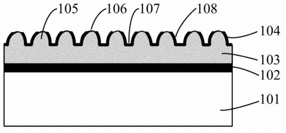
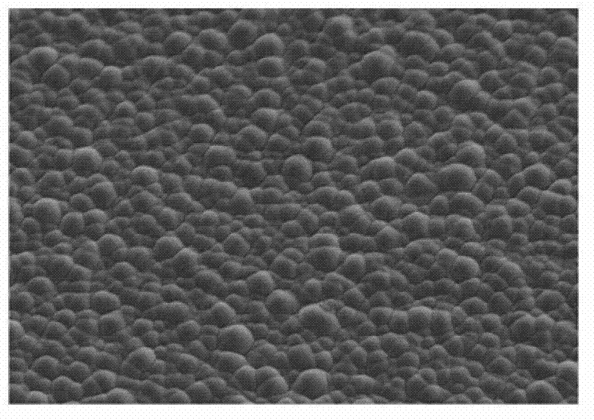
[0040] like figure 1 As shown, the thermal oxidation technology is used to grow and etch the isolation layer 102 on the substrate 101, and the substrate 101 is made of single crystal silicon; The thickness is 5000?; the polysilicon layer 103 with a thickness of 2 μm is grown by LPCVD technology. The temperature of the furnace tube for preparing the polysilicon layer 103 by LPCVD method is 620° C., the pressure is 300 mTorr, and the silane flow rate is 100 sccm (standard-state cubic centimeter per minute), Due to the large thickness of the polysilicon layer 103 , nano-bulges 105 are formed on the surface thereof, thus presenting a rough surface. A side wall material layer 104 with a thickness of 2000 ? is grown on the polysilicon layer 103 by LPCVD technology. During the deposition process, a TEOS (Tetraethyl Orthosilicate) source is used. The source temperature is 50°C and the furnace tube temperature is 720°C , the pressure is 300mTorr, O 2 The flow rate is 200 sccm. Becau...

Embodiment 2

[0045] like figure 1 As shown, on the substrate 101, PECVD (plasma enhanced chemical vapor deposition) technology is used to grow and etch the isolation layer 102, and the PECVD deposits and grows SiO 2 The temperature of the furnace tube is 270°C, the power is 103W, the pressure is 250mTorr, the silane flow rate is 300sccm, accounting for 4.6% of the total gas, N 2 The flow rate of O is 150 sccm, and the thickness of the etching isolation layer 102 is 5000 Å; the polysilicon layer 103 with a thickness of 1.5 μm is grown by PECVD technology, and the furnace tube temperature of the PECVD polysilicon layer 103 is 270°C, the power is 170W, the pressure is 400mTorr, and silane SiH 4 The flow rate is 300 sccm, because the thickness of the polysilicon layer 103 is relatively large, nano-bulges 105 are formed on its surface, so the surface is rough; on the polysilicon layer 103, a side wall material layer 104 with a thickness of 1500 Å is grown by PECVD, and the side wall is grown b...

Embodiment 3

[0050] like figure 1 As shown, a polysilicon layer 103 with a thickness of 2 μm is directly grown on the substrate 101 by LPCVD technology. The furnace tube temperature of the LPCVD polysilicon layer 103 is 620° C., the pressure is 300 mTorr, and the flow rate of silane is 100 sccm. Since the polysilicon layer 103 is relatively thick, Nano bulges 105 are formed on its surface, so the surface is rough; on the polysilicon layer 103, a side wall material layer 104 with a thickness of 2000 ? 720°C, the furnace tube pressure is 300mTorr, O 2 The flow rate is 200 sccm. Because of the existence of the nano-bulge 105, the sidewall material layer 104 forms SiO on the sidewall of the nano-bulk 105. 2sidewall 108, and the SiO 2 The thinnest, SiO in the first gap 107 of the nanobulge 105 2 thickest.

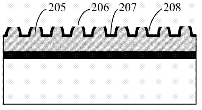
[0051] like image 3 As shown, the silicon substrate grown with two layers of material was put into RF power of 350W, Cl 2 In the cavity of the reactive ion etching machine with the H...


PUM

PropertyMeasurementUnit
Bottom diameteraaaaaaaaaa

Abstract

The invention relates to a machining method of a nano column/needle forest structure and belongs to the technical field of a semiconductor. According to the technical scheme provided by the invention, the machining method of the nano column/needle forest structure comprises the following steps of a, preparing and cleaning a selected substrate; b, growing a layer of polysilicon on the substrate; c, growing a spacer material layer on the substrate on which the polysilicon is grown, wherein the spacer material layer is coated on the polysilicon layer; d, performing anisotropic etching of the polysilicon on the substrate on which the spacer material layer and the polysilicon layer are coated; and e, adjusting the time of anisotropic etching until the required nano column/needle forest structure is formed. The limit of electronic beam photoetching and focused ion beam etching technology in the aspect of batch machining can be effectively overcome, the process complexity degree can be effectively reduced, and a large-area or patterned nano structure with high adjustability and uniformity is realized.

Description

technical field [0001] The invention relates to the field of nanostructure processing, in particular to a nanocolumn / needle forest structure processing method, which belongs to the technical field of semiconductors. Background technique [0002] Large-area nanopillar / needle structure, due to its structural characteristics such as large surface-to-volume ratio, large roughness, large surface area, tip, multi-pore / slit, etc., it presents super-hydrophilic / hydrophobic, enhanced plasmon oscillation, field emission, light filtering, Light absorption and other properties are often applicable to microfluidic devices, surface-enhanced Raman scattering devices, biomedical detection or functional devices, optoelectronic devices, optical sensor devices, new energy devices, etc., so it has gradually become one of the research hotspots in recent years. In many cases, the large-area, high-density nanopillar / needle structure looks like a dense forest, so it is also called the nanopillar / ne...

Claims


Application Information

Patent Timeline
IPC IPC(8): H01L21/3065H01L21/306B82Y40/00
Inventor 毛海央陈媛婧欧文谭振新
Owner 北京中科微知识产权服务有限公司
Why Eureka
Try Eureka