Epitaxial structure of high-brightness light emitting diode and implementation method thereof

A technology of light-emitting diodes and epitaxial structures, applied in electrical components, circuits, semiconductor devices, etc., can solve the technical difficulties of theoretically feasible epitaxial growth, increase non-radiative recombination of quantum wells, and low quantum efficiency in LEDs, and achieve improved radiation recombination Efficiency, enhanced radiative recombination probability, improved luminous efficiency and the effect of comprehensive device performance

Active Publication Date: 2012-12-19
YANGZHOU ZHONGKE SEMICON LIGHTING
View PDF4 Cites 26 Cited by
  • Summary
  • Abstract
  • Description
  • Claims
  • Application Information

AI Technical Summary

Problems solved by technology

Because there is usually a large lattice constant mismatch and thermal expansion coefficient difference between nitride and sapphire substrates, there are many crystal defects in the nitride epitaxial layer grown by metal organic chemical vapor deposition (MOCVD) epitaxy, such as Dislocations, etc., the crystal quality of the material is greatly affected
In particular, due to the polarization effect caused by the stress caused by the lattice mismatch between InGaN and GaN in the quantum well, there is a large polarization electric field in the quantum well, which leads to the spatial separation of electron and hole wave functions, and reduces the radiation recombination efficiency. , leading to low internal quantum efficiency of LEDs
At the same time, due to the high compressive stress in InGaN, the solid s...

Method used


Image

  • Epitaxial structure of high-brightness light emitting diode and implementation method thereof
  • Epitaxial structure of high-brightness light emitting diode and implementation method thereof
  • Epitaxial structure of high-brightness light emitting diode and implementation method thereof

Examples


Embodiment Construction

[0031] Using MOCVD equipment (CCS model Crius I 31 pieces commercial machine of Aixtron Company), the source of group V used is ammonia (NH3), and the organic source material of group III used to grow GaN and its alloys except the quantum well light-emitting region is Trimethylgallium (TMGa), trimethylaluminum (TMAl), the organic raw materials used to grow the quantum well active region are triethylgallium (TEGa), trimethylindium (TMIn), P-type doping using metal organics The source diphenocene magnesium (Cp2Mg) provides Mg impurity atoms, and N-type doping uses gaseous silane (SiH4) diluted with H2 to provide Si impurity atoms.

[0032] Combine below figure 1 , 2 Further illustrate the present invention:

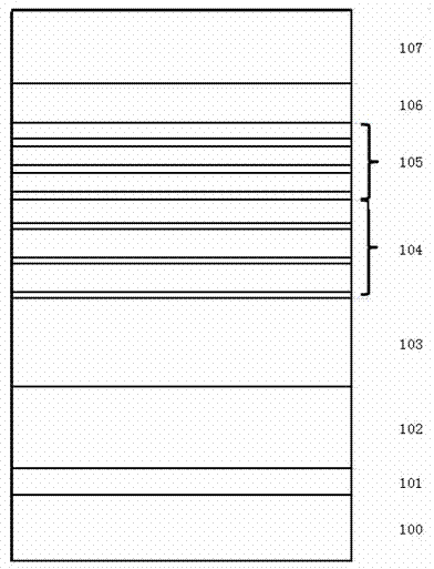
[0033] 1. Grow a layer of GaN low-temperature buffer layer 101 on the sapphire substrate 100: the growth temperature is 580°C, the pressure is 65000Pa, the thickness is 30nm, and the growth atmosphere is H 2 .

[0034] 2. A layer of unintentionally doped GaN layer 102 ...


PUM

PropertyMeasurementUnit
Thicknessaaaaaaaaaa
Thicknessaaaaaaaaaa

Abstract

An epitaxial structure of a high-brightness light emitting diode and an implementation method thereof belong to the technical field of semiconductor production. At least three pairs of coupled quantum wells grow. When each pair of coupled quantum wells grow, firstly, quantum well layers low in In content grow; and secondly, luminous quantum well layers grow, In content of each quantum well layer low in In content gradually increases along the growth direction, and a thin GaN barrier layer grows between each adjacent quantum well layer low in In content and luminous quantum well layer. A coupled quantum well structure which is low in In content and gradually increases in composition grows before a luminous quantum well by a variable temperature and variable precursor flow method, and accordingly a quantum well low in In content cannot adsorb photons emitted by the quantum well again, built-in electric field can be lowered, localization of carriers is enhanced to increase radiative recombination rate, and internal quantum efficiency of the light emitting diode is improved greatly.

Description

technical field [0001] The invention belongs to the technical field of semiconductor production, in particular to an epitaxial structure of a light emitting diode and a growth method thereof. Background technique [0002] Gallium Nitride (GaN) is the third generation direct energy gap wide bandgap semiconductor with a bandgap width of 3.39eV. GaN-based green and blue light-emitting diodes (LEDs) have the advantages of high brightness, low energy consumption, long life, and fast response, and are widely used in full-color display, signal indication, and landscape lighting. In particular, the research and development of white LEDs made of GaN-based blue LEDs mixed with phosphors is progressing rapidly. The emission wavelength of white LEDs is only in the visible light region, which avoids the strong infrared radiation of incandescent lamps and can save a lot of energy. At the same time, white LEDs are small in size, long in life, safe, efficient, and free of harmful substance...

Claims


Application Information

Patent Timeline
IPC IPC(8): H01L33/06H01L33/32H01L33/00
Inventor 李志聪李鸿渐李盼盼李璟孙一军王国宏
Owner YANGZHOU ZHONGKE SEMICON LIGHTING
Why Eureka
Try Eureka