Tri-strain tri-polycrystal-plane BiCMOS (Bipolar complementary metal oxide semiconductor) integrated device and preparation method thereof

An integrated device and three-strain technology, applied in semiconductor/solid-state device manufacturing, electric solid-state devices, semiconductor devices, etc., can solve problems such as incompatibility, complicated preparation process, and poor heat dissipation performance

Inactive Publication Date: 2013-01-09
XIDIAN UNIV
View PDF2 Cites 0 Cited by
  • Summary
  • Abstract
  • Description
  • Claims
  • Application Information

AI Technical Summary

Problems solved by technology

Although the frequency characteristics of GaAs and InP-based compound devices are superior, their preparation process is more complicated than Si process, the cost is high, the preparation of large diameter single crystal is difficult, the mechanical strength is low, the heat dissipation performance is not good, it is difficult to be compatible with Si process, and it lacks SiO2. Factors such as passivation layer limit its wide application and development
[0007] Due to the low mobility of Si materials, the performance of integrated circuits manufactured by Si BiCMOS technology, especially the frequency performance, is greatly limited; for SiGe BiCMOS technology, although SiGe HBT is used for bipolar transistors, However, Si CMOS is still used for unipolar devices that restrict the improvement of the frequency characteristics of BiCMOS integrated circuits, so these limit the further improvement of the performance of BiCMOS integrated circuits

Method used


Image

  • Tri-strain tri-polycrystal-plane BiCMOS (Bipolar complementary metal oxide semiconductor) integrated device and preparation method thereof

Examples


Embodiment 1

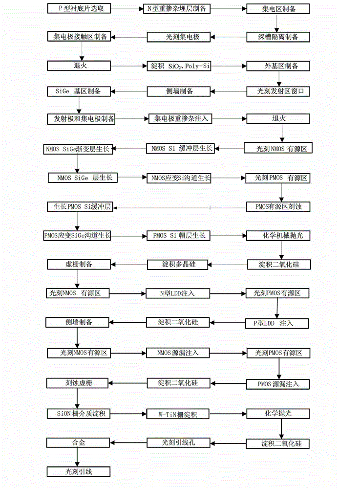
[0124] Embodiment 1: Preparation of a three-strain, three-polycrystalline planar BiCMOS integrated device and circuit with a 45nm conductive channel, the specific steps are as follows:

[0125] Step 1, epitaxial growth.

[0126] (1a) Choose the doping concentration as 5×10 14 cm -3 P-type Si wafer as the substrate;

[0127] (1b) Thermally oxidize a layer of SiO with a thickness of 300nm on the surface of the substrate 2 Floor;

[0128] (1c) Photoetching the buried region, implanting N-type impurities in the buried region, and annealing at 800°C for 90 min to activate the impurities to form an N-type heavily doped buried region.

[0129] Step 2. Preparation of isolation area.

[0130] (2a) Remove the excess oxide layer on the surface, and epitaxially grow a layer with a doping concentration of 1×10 16 cm -3 The Si layer with a thickness of 2μm serves as a collector area;

[0131] (2b) Thermally oxidize a layer of SiO with a thickness of 300nm on the surface of the substrate 2 Floor;

[0132...

Embodiment 2

[0193] Embodiment 2: Preparation of a three-strain, three-polycrystalline planar BiCMOS integrated device and circuit with a conductive channel of 30 nm, the specific steps are as follows:

[0194] Step 1, epitaxial growth.

[0195] (1a) Choose the doping concentration as 1×10 15 cm -3 P-type Si wafer as the substrate;

[0196] (1b) Thermally oxidize a layer of SiO with a thickness of 400nm on the surface of the substrate 2 Floor;

[0197] (1c) Photoetching the buried region, implanting N-type impurities in the buried region, and annealing at 900°C for 60 minutes to activate the impurities to form an N-type heavily doped buried region.

[0198] Step 2. Preparation of isolation area.

[0199] (2a) Remove the excess oxide layer on the surface, and epitaxially grow a layer with a doping concentration of 5×10 16 cm -3 The Si layer with a thickness of 2.5μm is used as a collector area;

[0200] (2b) Thermally oxidize a layer of SiO with a thickness of 400nm on the surface of the substrate 2 Fl...

Embodiment 3

[0262] Embodiment 3: Preparation of a three-strain, three-polycrystalline planar BiCMOS integrated device and circuit with a 22nm conduction channel, the specific steps are as follows:

[0263] Step 1, epitaxial growth.

[0264] (1a) Choose the doping concentration as 5×10 15 cm -3 P-type Si wafer as the substrate;

[0265] (1b) Thermal oxidation of a layer of SiO with a thickness of 500nm on the surface of the substrate 2 Floor;

[0266] (1c) Photoetching the buried region, implanting N-type impurities in the buried region, and annealing at 950°C for 30 minutes to activate the impurities to form an N-type heavily doped buried region.

[0267] Step 2. Preparation of isolation area.

[0268] (2a) Remove the excess oxide layer on the surface, and epitaxially grow a layer with a doping concentration of 1×10 17 cm -3 The Si layer with a thickness of 3μm is used as a collector area;

[0269] (2b) Thermally oxidize a layer of SiO with a thickness of 500nm on the surface of the substrate 2 Floor...


PUM

PropertyMeasurementUnit
thicknessaaaaaaaaaa
thicknessaaaaaaaaaa
thicknessaaaaaaaaaa

Abstract

The invention discloses a tri-strain tri-polycrystal-plane BiCMOS (Bipolar complementary metal oxide semiconductor) integrated device and a preparation method thereof. The method comprises the following steps: preparing an embedded layer on a substrate plate, growing N-type Si epitaxy, preparing a deep channel isolator, preparing a collecting electrode contact area, preparing a base area and a transmission area, and forming a SiGe HBT (Heterojunction bipolar transistor) device; etching deep channels in the active areas of an NMOS (N-channel metal oxide semiconductor) device and a PMOS (P-channel metal oxide semiconductor) device, selectively epitaxially growing the following layers in the channel: a P-type Si layer, a P-type SiGe gradient layer, a P-type SiGe layer, a P-type strain Si layer as the active area of the NMOS device, an N-type Si layer, an N-type strain SiGe layer, and an N-type Si cap layer as the active area of the PMOS device; preparing a virtual grid, performing MOS (Metal oxide semiconductor) device light doped source / drain (LDD) injection, preparing a spacer, and self-aligning to form an MOS device source / drain; and etching the virtual grid, and sedimentating an SiON grid dielectric layer and a W-TiN composite grid to form a CMOS structure, and finally forming a BiCMOS circuit. According to the method, a tensile strain Si with high electron mobility and a compressive strain SiGe with high hole mobility are fully utilized as the conductive channels of the NMOS device and the PMOS device respectively, thus the performances of a BiCMOS integrated circuit are effectively improved.

Description

Technical field [0001] The invention belongs to the technical field of semiconductor integrated circuits, and in particular relates to a three-strain, three-polycrystalline planar BiCMOS integrated device and a preparation method. Background technique [0002] The integrated circuit that appeared in 1958 is one of the most influential inventions of the 20th century. Based on this invention, microelectronics has become the basis of existing modern technology, accelerating the change of the knowledge and informationization of human society, and also changing the way of thinking of human beings. It not only provides a powerful tool for mankind to transform nature, but also opens up a broad space for development. [0003] Semiconductor integrated circuits have become the foundation of the electronics industry, and people's huge demand for the electronics industry has promoted the rapid development of this field. In the past few decades, the rapid development of the electronics indust...

Claims


Application Information

Patent Timeline
Patent Type & Authority Applications(China)
IPC IPC(8): H01L27/06H01L21/28H01L21/8249
Inventor 胡辉勇宋建军宣荣喜舒斌张鹤鸣李妤晨吕懿郝跃
Owner XIDIAN UNIV
Why Eureka
Try Eureka