Method for electrochemically preparing thermoelectric film by using seeding layer
A thermoelectric thin film and electrochemical technology, applied in the field of electrochemical preparation of thermoelectric thin films on the seed layer, can solve problems such as poor bonding, and achieve the effects of high deposition rate, low growth temperature, and low cost
- Summary
- Abstract
- Description
- Claims
- Application Information
AI Technical Summary
Problems solved by technology
Method used
Image

Examples
Embodiment 1
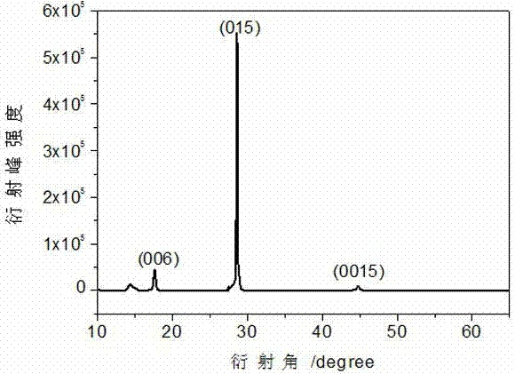
[0023] Embodiment one: Constant current deposition seed layer on the glass sheet, then constant potential growth Bi 2 Te 3
[0024] Cleaning of glass slides: First, clean manually with cotton dipped in detergent, then ultrasonically clean with water containing detergent for 10 minutes, then ultrasonically clean with ultrapure water for 5 minutes to remove residual detergent, then ultrasonically clean with acetone and absolute ethanol for 10 minutes minute. Dry it with high-purity N2 and put it into the sample box for later use.
[0025] Use constant current deposition as the preparation of the seed layer, the specific parameters are: current density 1mA / cm 2 , the deposition time is 2 minutes, and the thickness of the obtained seed layer is about 100m.
[0026] The solution used for electrochemical growth was Bi(NO 3 ) 3· 5H 2O, at a concentration of 0.008 M / L; TeO 2 , the concentration is 0.01 M / L; HNO 3 The concentration is 1M / L. The deposition potential ...
Embodiment 2
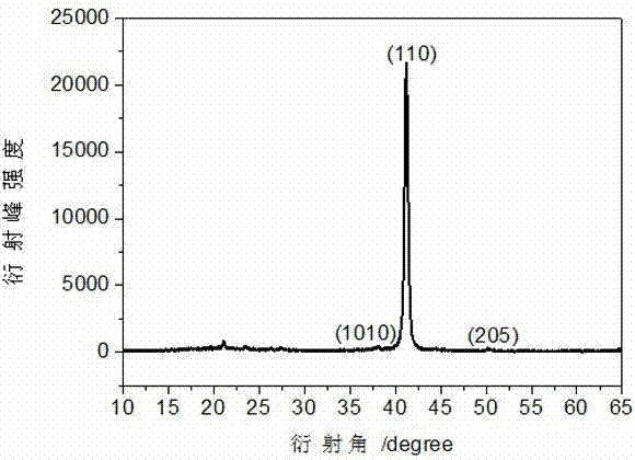
[0027] Embodiment two: silicon substrate magnetron sputtering seed layer, then constant potential growth Bi 2 Te 3
[0028] Cleaning of silicon substrate: use RCA chemical cleaning process to clean, the specific steps are: first in liquid A (H 2 O:H 2 o 2 :NH 3 h 2 O=5:1:1) in an 80°C water bath for 10 minutes, then in solution B (HCl:H 2 0 2 :H 2 0=1:1:6) in 80°C water bath for 10min, then in liquid C BOE (HF:NH 4 Soak in F=1:6) for 5 minutes, and finally rinse with a large amount of deionized water, ultra-pure N 2 Blow dry and store in sample box.
[0029] The specific parameters for the preparation of the seed layer by magnetron sputtering are: the co-sputtering method of Bi target and Te target is used, and the background vacuum is less than 2*10 -6 torr, the sputtering working gas is high-purity argon with a purity of 99.999%, the working pressure of argon is 1.5mTorr, the sputtering power of the Bi target is 15 w, the sputtering power of the Te target...
Embodiment 3
[0031] Example 3: Molecular beam epitaxy deposits a seed layer on a glass sheet, and then grows Bi at a constant potential 2 Te 3
[0032] Cleaning of glass slides: First, clean manually with cotton dipped in detergent, then ultrasonically clean with water containing detergent for 10 minutes, then ultrasonically clean with ultrapure water for 5 minutes to remove residual detergent, then ultrasonically clean with acetone and absolute ethanol for 10 minutes minute. With high purity N 2 Blow dry and put into the sample box for later use.
[0033] The seed layer is grown by molecular beam epitaxy, and the specific parameters are: the degree of vacuum is 3*10 -7 pa, the temperature of the glass sheet is 200°C, the temperature of the Bi beam source furnace is 490°C, the temperature of the Te beam source furnace is 280°C, the epitaxy time is 20 minutes, and the obtained film thickness is 30nm.
[0034] Electrochemical growth, the selected solution is Bi(NO 3 ) 3· 5H 2...
PUM
| Property | Measurement | Unit |
|---|---|---|
| Thickness | aaaaa | aaaaa |
| Thickness | aaaaa | aaaaa |
Abstract
Description
Claims
Application Information
 - R&D
- Intellectual Property
- Life Sciences
- Materials
- Tech Scout
- Unparalleled Data Quality
- Higher Quality Content
- 60% Fewer Hallucinations
Browse by: Latest US Patents, China's latest patents, Technical Efficacy Thesaurus, Application Domain, Technology Topic, Popular Technical Reports.
© 2025 PatSnap. All rights reserved.Legal|Privacy policy|Modern Slavery Act Transparency Statement|Sitemap|About US| Contact US: help@patsnap.com