

Semiconductor film with gradually increased hole diameters of different layers and preparation method thereof
A semiconductor and aperture technology, applied in the field of dye-sensitized solar cells, can solve the problems of reducing the overall specific surface area of the photoanode, affecting the dye adsorption amount, etc., and achieves good light scattering effect, improves the utilization rate of incident light, and is easy to obtain.
- Summary
- Abstract
- Description
- Claims
- Application Information
AI Technical Summary
Problems solved by technology
Method used
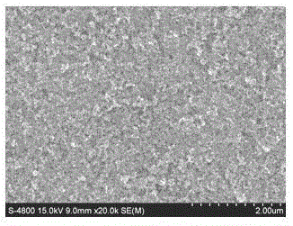
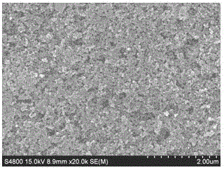
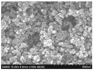
Image

Examples
Embodiment 1
[0025] First, weigh 10g of styrene monomer, 0.13g of potassium persulfate, and 1g of polyvinylpyrrolidone-K30, add the mixture of the three into 100ml of deionized water, and 80 o C was refluxed for 6 hours to prepare polystyrene microspheres with a particle diameter of 200 nm.
[0026] Weigh 4g of terpineol, 20g of absolute ethanol, 1g of P25, 0.3g of ethyl cellulose and 60g of zirconium beads, and mix them by ball milling for 2 hours. After the ball milling, remove the ethanol with a rotary evaporator to prepare the bottom layer slurry of the semiconductor film.
[0027] Weigh 0.25g of the above-prepared polystyrene microspheres, 4g of terpineol, 20g of absolute ethanol, 1g of P25, 0.3g of ethyl cellulose and 60g of zirconium beads, mix them by ball milling for 2 hours, and remove them with a rotary evaporator after ball milling. Ethanol to prepare the interlayer slurry on the bottom layer of the semiconductor film.
[0028] Weigh 0.5g of the above-prepared polystyrene micr...
Embodiment 2
[0031] Weigh 4g of terpineol, 20g of absolute ethanol, 1g of P25, 0.3g of ethyl cellulose and 60g of zirconium beads, and mix them by ball milling for 2 hours. After the ball milling, remove the ethanol with a rotary evaporator to prepare the bottom layer slurry of the semiconductor film.
[0032] Weigh 0.25g of the above-prepared polystyrene microspheres, 4g of terpineol, 20g of absolute ethanol, 1g of P25, 0.3g of ethyl cellulose and 60g of zirconium beads, mix them by ball milling for 2 hours, and remove them with a rotary evaporator after ball milling. Ethanol to prepare the interlayer slurry on the bottom layer of the semiconductor film.
[0033]Weigh 0.5g of the above-prepared polystyrene microspheres, 4g of terpineol, 20g of absolute ethanol, 1g of P25, 0.3g of ethyl cellulose and 60g of zirconium beads, mix them by ball milling for 2 hours, and remove them with a rotary evaporator after ball milling. Ethanol to prepare the top layer slurry on the middle layer of the se...
Embodiment 3
[0036] Weigh 5g of terpineol, 25g of absolute ethanol, 1g of P25, 0.5g of ethyl cellulose and 60g of zirconium beads, and mix them by ball milling for 3 hours. After the ball milling, remove the ethanol with a rotary evaporator to prepare the bottom layer slurry of the semiconductor film.
[0037] Weigh 0.25g of the above-prepared polystyrene microspheres, 5g of terpineol, 25g of absolute ethanol, 1g of P25, 0.5g of ethyl cellulose and 60g of zirconium beads, mix them by ball milling for 3 hours, and remove them with a rotary evaporator after ball milling. Ethanol to prepare the interlayer slurry on the bottom layer of the semiconductor film.
[0038] Weigh 0.5g of the above-prepared polystyrene microspheres, 5g of terpineol, 25g of absolute ethanol, 1g of P25, 0.5g of ethyl cellulose and 60g of zirconium beads, mix them by ball milling for 3 hours, and remove them with a rotary evaporator after ball milling. Ethanol to prepare the top layer slurry on the middle layer of the s...
PUM
| Property | Measurement | Unit |
|---|---|---|
| Diameter | aaaaa | aaaaa |
Abstract
Description
Claims
Application Information