Active matrix organic light emitting diode driving back plate and preparation method of active matrix organic light emitting diode driving back plate

A technology for light-emitting diodes and driving backplanes, which is applied in semiconductor/solid-state device manufacturing, electric solid-state devices, semiconductor devices, etc., can solve the problems of unfavorable promotion and use, complicated manufacturing process, and high production cost, and achieve good industrial application value , Reduce the number of photomasks and improve the yield rate

Inactive Publication Date: 2013-02-27
GUANG ZHOU NEW VISION OPTO ELECTRONICS TECH
View PDF1 Cites 23 Cited by
  • Summary
  • Abstract
  • Description
  • Claims
  • Application Information

AI Technical Summary

Problems solved by technology

However, the manufacturing process of existing metal oxide semiconductor materials is complicated and the production cost is high, which is not conducive to the popularization and use of metal oxide semiconductor materials in the production of drive backplanes.

Method used


Image

  • Active matrix organic light emitting diode driving back plate and preparation method of active matrix organic light emitting diode driving back plate
  • Active matrix organic light emitting diode driving back plate and preparation method of active matrix organic light emitting diode driving back plate
  • Active matrix organic light emitting diode driving back plate and preparation method of active matrix organic light emitting diode driving back plate

Examples


Embodiment 1

[0061] A method for preparing an active matrix organic light-emitting diode driving backplane includes the following steps.

[0062] Firstly, a metal conductive layer is deposited and patterned on the substrate as a gate metal layer.

[0063] The metal used to prepare the gate metal layer can be: aluminum (Al), copper (Cu), molybdenum (Mo), titanium (Ti), silver (Ag), gold (Au), tantalum (Ta), chromium ( Cr) at least one of the simple substances or aluminum alloy. Usually, the above metal materials are deposited on the substrate by physical vapor deposition PVD (Physical Vapor Deposition) method to form a metal conductive layer.

[0064] The thickness of the metal conductive layer is 100nm to 2000nm. The metal conductive layer can be a single-layer metal film or a multi-layer film composed of a single-layer metal film. The single-layer metal film is any one of aluminum film, copper film, molybdenum film, titanium film, silver film, gold film, tantalum film, chromium film or...

Embodiment 2

[0091] A method for preparing an active matrix organic light-emitting diode driving backplane includes the following steps.

[0092] Such as figure 1 shown, in a SiO with 200 nm thick 2On the alkali-free glass substrate 1 of the buffer layer 2, a layer of Mo metal film with a thickness of 25 nm was deposited using PVD physical vapor deposition method, and then a layer of Al metal film with a thickness of 100 nm was deposited, and then a layer of Al metal film with a thickness of 25 nm was deposited. Mo metal film, three layers of metal film constitute the metal layer.

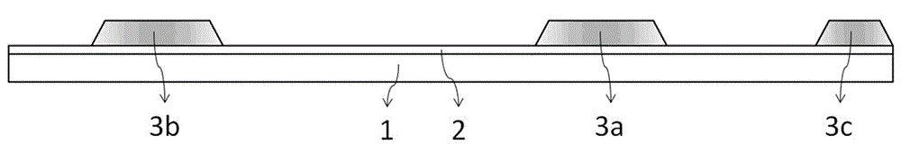
[0093] Then, the metal layer is patterned by a photolithography process to form a gate metal layer, and the gate metal layer is respectively used as a gate, a lower electrode of a capacitor, and a signal wire. figure 1 Among them, 3a is the gate of the thin film transistor, 3b is the lower electrode substrate of the storage capacitor, and 3c is the contact hole required for wiring between metal layers.

[00...

Embodiment 3

[0104] Such as figure 1 shown in a 50 nm thick Si 3 N 4 On the alkali-free glass substrate 1 of the buffer layer 2, Mo and Cu metal films are sequentially deposited by PVD method as the grid, the lower electrode of the capacitor and the signal wire. The thicknesses of the Mo and Cu metal films are 25 nm and 200 nm, respectively. Use a photolithography process to pattern it to form a metal layer, where 3a is the gate of the thin film transistor, 3b is the lower electrode plate of the storage capacitor, and 3c is the contact hole required for the wiring between the metal layers.

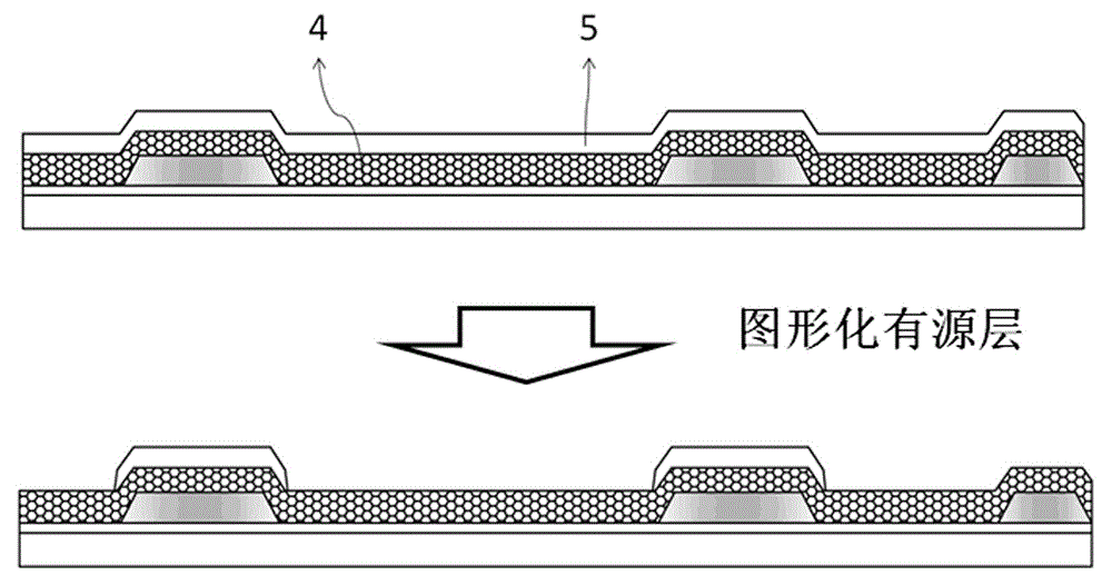
[0105] Such as figure 2 As shown, on the patterned gate metal, use PVD equipment to deposit Si with a thickness of 400 nm by reactive sputtering 3 N 4 As the gate insulating layer 4, then continue to deposit 30 nm metal oxide IZZO (In, Zn, Zr atomic ratio 1:1:0.1) as the active layer 5 without breaking the vacuum. Use Ruihong 304 photoresist as a photolithography mask, use dilute hydrochloric aci...


PUM

PropertyMeasurementUnit
thicknessaaaaaaaaaa
thicknessaaaaaaaaaa
thicknessaaaaaaaaaa

Abstract

The invention relates to an active matrix organic light emitting diode driving back plate and a preparation method of the active matrix organic light emitting diode driving back plate. The preparation method comprises the steps that a metal conducting layer is deposited and patterned on a substrate to be used as a grid electrode metal layer; an insulating film is deposited on the grid electrode metal layer to be used as a grid electrode insulating layer; a metal oxide film is deposited and patterned on the grid electrode insulating layer to be used as an active layer; another insulating film is deposited on the active layer to be used as an etching barrier layer; contact holes, the effective area of a memory capacitor and a source drain electrode region of a film transistor are patterned and defined on the etching barrier layer; and a conducting film is deposited and patterned on the etching barrier layer to be used as a source drain electrode layer of the film transistor. The memory capacitor uses the grid electrode metal layer as a lower electrode plate, uses the grid electrode insulating layer as a dielectric layer and uses the active source as a protecting layer of the grid electrode insulating layer, the effective area of the capacitor is defined by the etching barrier layer, and in addition, the conducting film layer is used as an upper electrode plate of the capacitor. The active matrix organic light emitting diode driving back plate and the preparation method have the characteristics that the preparation process is simple, and the cost is low. The important industry application value technology is realized.

Description

technical field [0001] The invention relates to the technical field of semiconductors, in particular to an active matrix organic light emitting diode driving backplane and a preparation method thereof. Background technique [0002] Thin Film Transistor (TFT, Thin Film Transistor) is currently mainly used to drive the sub-pixels of Liquid Crystal Display (LCD, Liquid Crystal Display) and Organic Light-Emitting Diode (OLED, Organic Light-Emitting Diode) displays. [0003] The driving backplane made of thin film transistor array is a key component for the display to achieve higher pixel density, aperture ratio and improved brightness. At present, TFTs to LCDs generally use a TFT backplane based on amorphous silicon as an active layer. [0004] However, due to the low mobility of amorphous silicon (a-Si) (usually 0.1cm 2 V -1 the s -1 left and right), which cannot satisfy OLED displays, and cannot be applied to the production of active matrix organic light-emitting diode (A...

Claims


Application Information

Patent Timeline
Patent Type & Authority Applications(China)
IPC IPC(8): H01L21/77H01L27/32
Inventor 徐苗罗东向庞佳威王琅周雷李民徐华彭俊彪
Owner GUANG ZHOU NEW VISION OPTO ELECTRONICS TECH
Why Eureka
Try Eureka