Adjustable film bulk acoustic wave resonator and preparation method thereof
A thin-film bulk acoustic wave and resonator technology, applied in impedance networks, electrical components, etc., can solve the problems of low tunability and large leakage current density of bulk acoustic wave resonators, and achieve low leakage current, improved leakage current, and suitable mediation. The effect of electric constant
- Summary
- Abstract
- Description
- Claims
- Application Information
AI Technical Summary
Problems solved by technology
Method used
Image

Examples
preparation example Construction
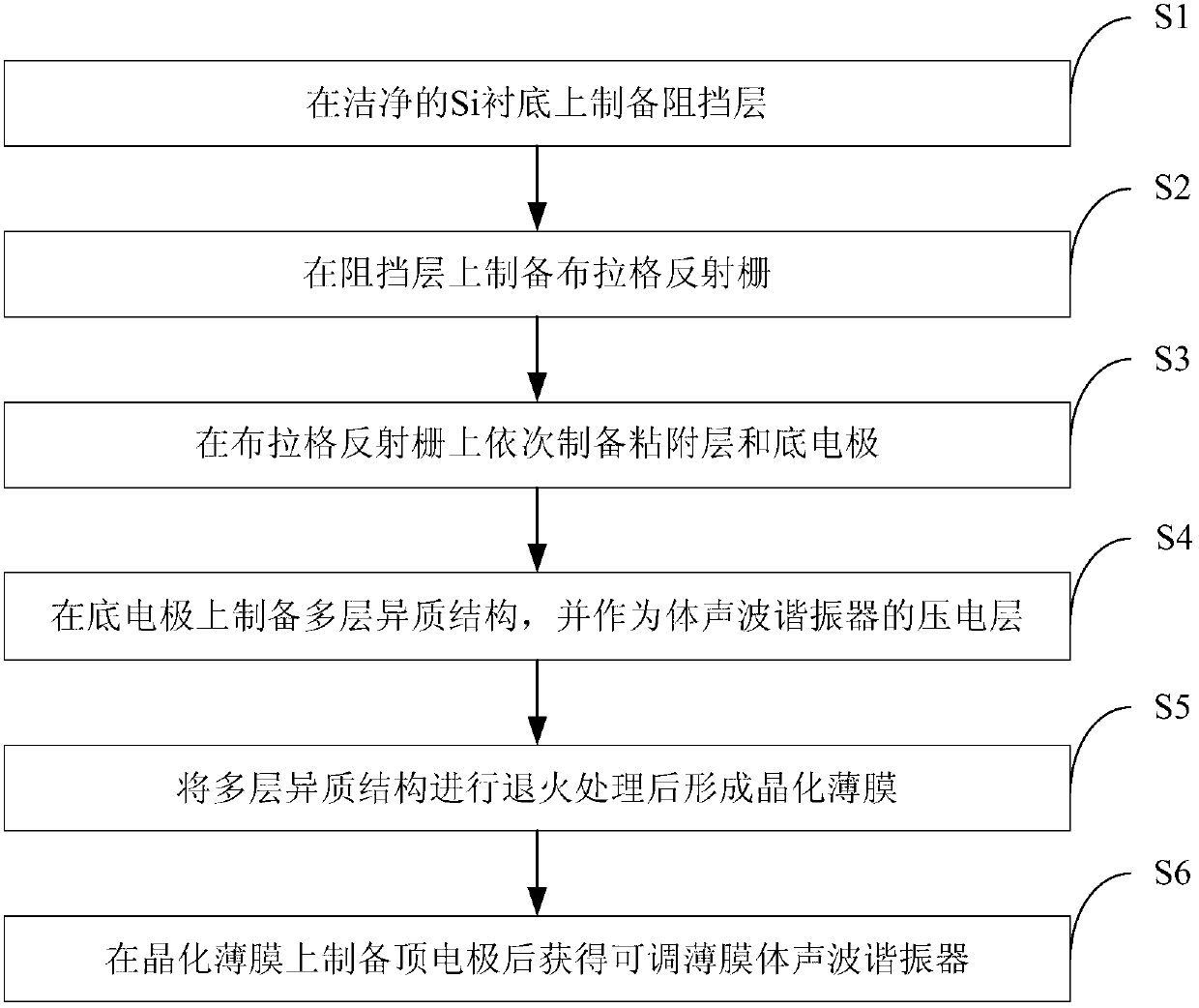
[0028] figure 1 It shows the implementation process of the preparation method of the tunable thin-film bulk acoustic resonator provided by the embodiment of the present invention, specifically including:
[0029] S1: preparing a barrier layer on a clean Si substrate;
[0030] S2: Fabricate a Bragg reflection grating on the barrier layer, and the Bragg reflection grating is composed of films with different acoustic impedances;
[0031] S3: sequentially prepare an adhesion layer and a bottom electrode on the Bragg reflection grating;
[0032] S4: sequentially prepare BST and BZT thin films on the bottom electrode to form BZT, BST and BZT or BST, BZT and BST multilayer heterostructure, and serve as the piezoelectric layer of the bulk acoustic wave resonator;
[0033] S5: annealing the BST and BZT films to form a crystallized film;
[0034] S6: A tunable thin-film bulk acoustic resonator is obtained after preparing the top electrode on the crystallized thin film.
[0035] In t...
Embodiment 1
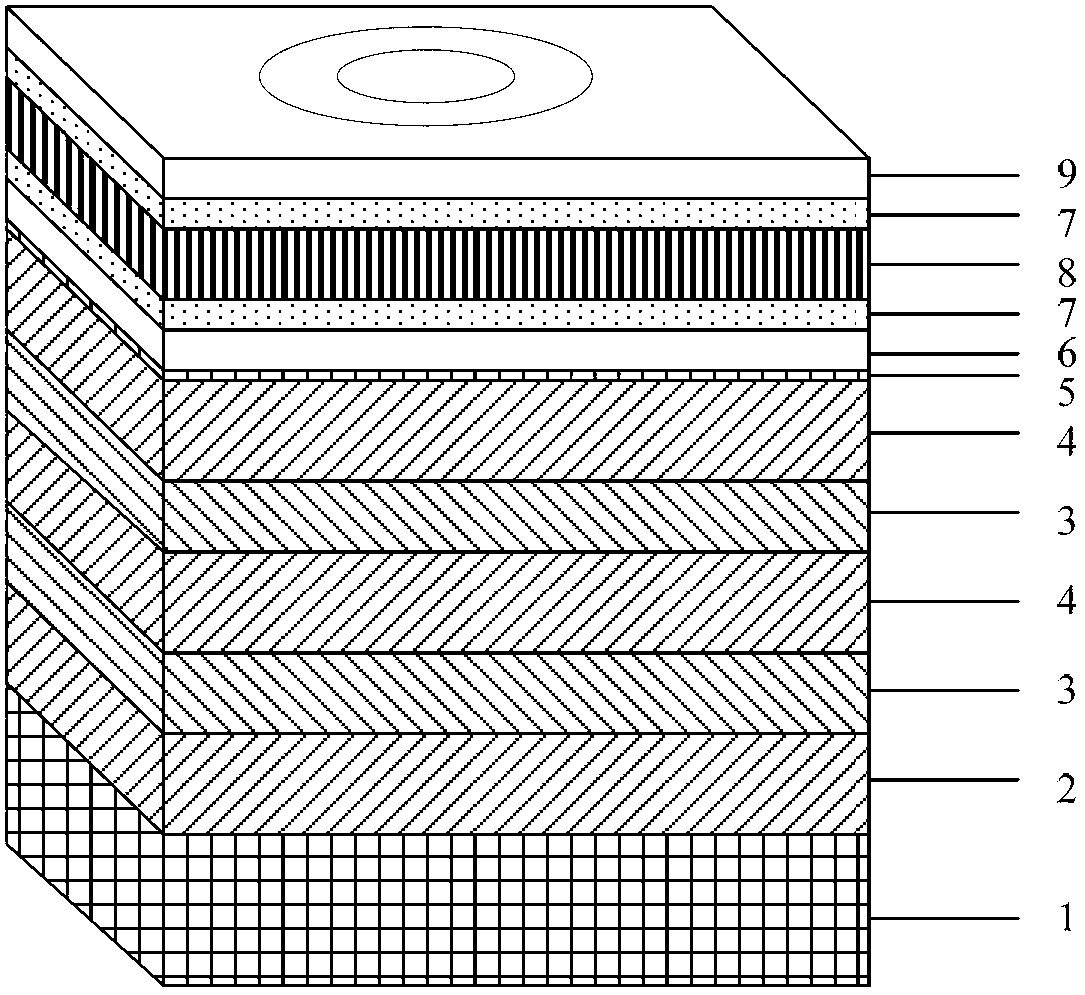
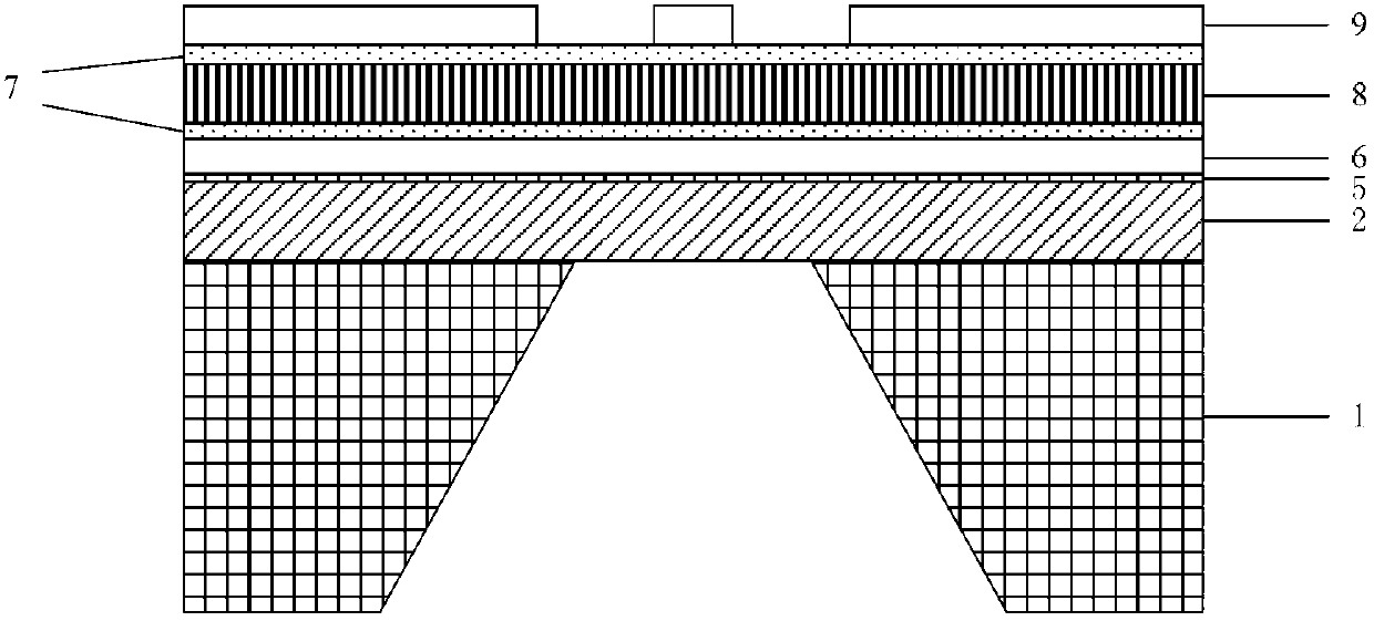
[0038] (1) A silicon wafer 1 with a crystal phase selected, with a thickness of 0.5 mm, was ultrasonically cleaned in toluene, acetone and absolute ethanol for 5 minutes, and dried with high-purity N2;
[0039] (2) prepare barrier layer 2 with the method for radio frequency magnetron sputtering, the material of barrier layer selects SiO for use;
[0040] (3) Prepare 3 and 4 thin films sequentially on the barrier layer 2 by radio frequency magnetron sputtering to obtain two pairs of Bragg reflection gratings composed of 3 and 4 epitaxial thin films, wherein 3 and 4 can be SiO2, W, SiO2 respectively , Mo or SiO2, Au, etc., the thickness of 3 and 4 is selected according to different materials;
[0041] (4) Prepare the adhesive layer 5 and the bottom electrode 6 successively on the above-prepared Bragg reflection grating with the method of radio frequency magnetron sputtering, wherein the adhesive layer is selected Ti or TiO2, and the bottom electrode is selected Pt or Au etc., a...
Embodiment 2
[0046] (1) A silicon wafer 1 with a crystal phase selected, with a thickness of 0.5 mm, was ultrasonically cleaned in toluene, acetone and absolute ethanol for 5 minutes, and dried with high-purity N2;
[0047] (2) Prepare barrier layer 2, adhesion layer 5 and bottom electrode 6 successively on 1 with the method of radio frequency magnetron sputtering, wherein barrier layer selects SiO2 for use, adhesion layer can select Ti or TiO2 for use, bottom electrode selects Pt or Au for use etc., whose thicknesses are 300nm, 20nm and 100nm respectively;
[0048] (3) Prepare 7 and 8 thin films successively by radio frequency magnetron sputtering to obtain a piezoelectric layer of a bulk acoustic wave resonator composed of 7, 8 and 7 three-layer epitaxial structures. The piezoelectric layer can be BZT, BST and BZT It can also be BST, BZT and BST. The thicknesses of 7 and 8 are 50nm and 200nm respectively. The sputtering parameters of 7 and 8 are: target base distance 70mm, working press...
PUM
| Property | Measurement | Unit |
|---|---|---|
| Thickness | aaaaa | aaaaa |
| Thickness | aaaaa | aaaaa |
| Outer diameter | aaaaa | aaaaa |
Abstract
Description
Claims
Application Information